鑫景福致力于滿足“快速服務,零缺陷,輔助研發(fā)”PCBA訂購單需求。


PCBA方案設計
What are the special importance of the circuit board design of the power supply
The Circuit board manufacturer, circuit board design and PCBA manufacturer will explain to you what is partICularly important about the circuit board design of the power supply
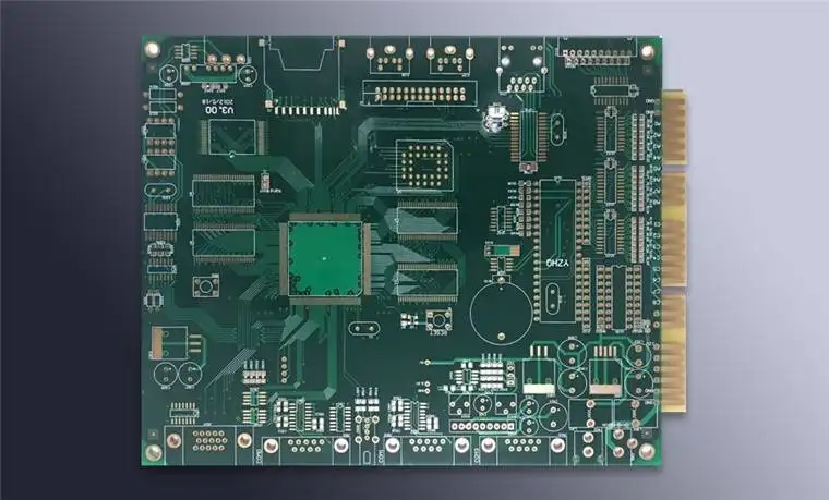
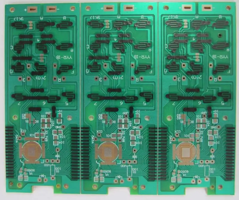
PCB circuit board is the basic electronic component of all electronic circuit design. As the main support, it carries all the components that make up the circuit. The role of PCB is not only to combine the scattered components, but also to ensure the regularity of circuit design, which can well avoid the confusion and errors caused by manual wiring and wiring.
This paper introduces the five key points of PCB design in power supply design in detail.
1. There should be a reasonable trend
Such as input/output, AC/DC, strong/weak signal, high frequency/low frequency, high voltage/low voltage, etc. Their strike should be linear (or separate), and should not blend with each other. Its purpose is to prevent mutual interference. The best trend is straight line, but it is generally not easy to achieve. The most unfavorable trend is circular. Fortunately, isolation can be set to improve. The requirements for DC, SMAll signal and low-voltage PCB design can be lower. So "reasonable" is relative.
2. Choose a good grounding point: the grounding point is often the most important
How many engineers and technicians have discussed the small grounding point? This shows its importance. In general, common grounding is required, for example, multiple ground wires of the forward amplifier shall be connected to the trunk ground after being converged. In reality, it is difficult to do it completely due to various restrictions, but we should try our best to follow them. This problem is quite flexible in practice. Everyone has his own set of solutions. It is easy to understand if he can explain it to specific circuit boards.
3. Reasonably arrange power filter/decoupling capacitor
Generally, only a few power supply filter/decoupling capacitors are drawn in the schematic diagram, but they are not indicated where they should be connected. In fact, these capacitors are set for switching devices (gate circuits) or other components requiring filtering/decoupling. These capacitors should be arranged as close to these components as possible, and will not work if they are too far away. Interestingly, when the power filter/decoupling capacitor is arranged properly, the problem of grounding point is less obvious.
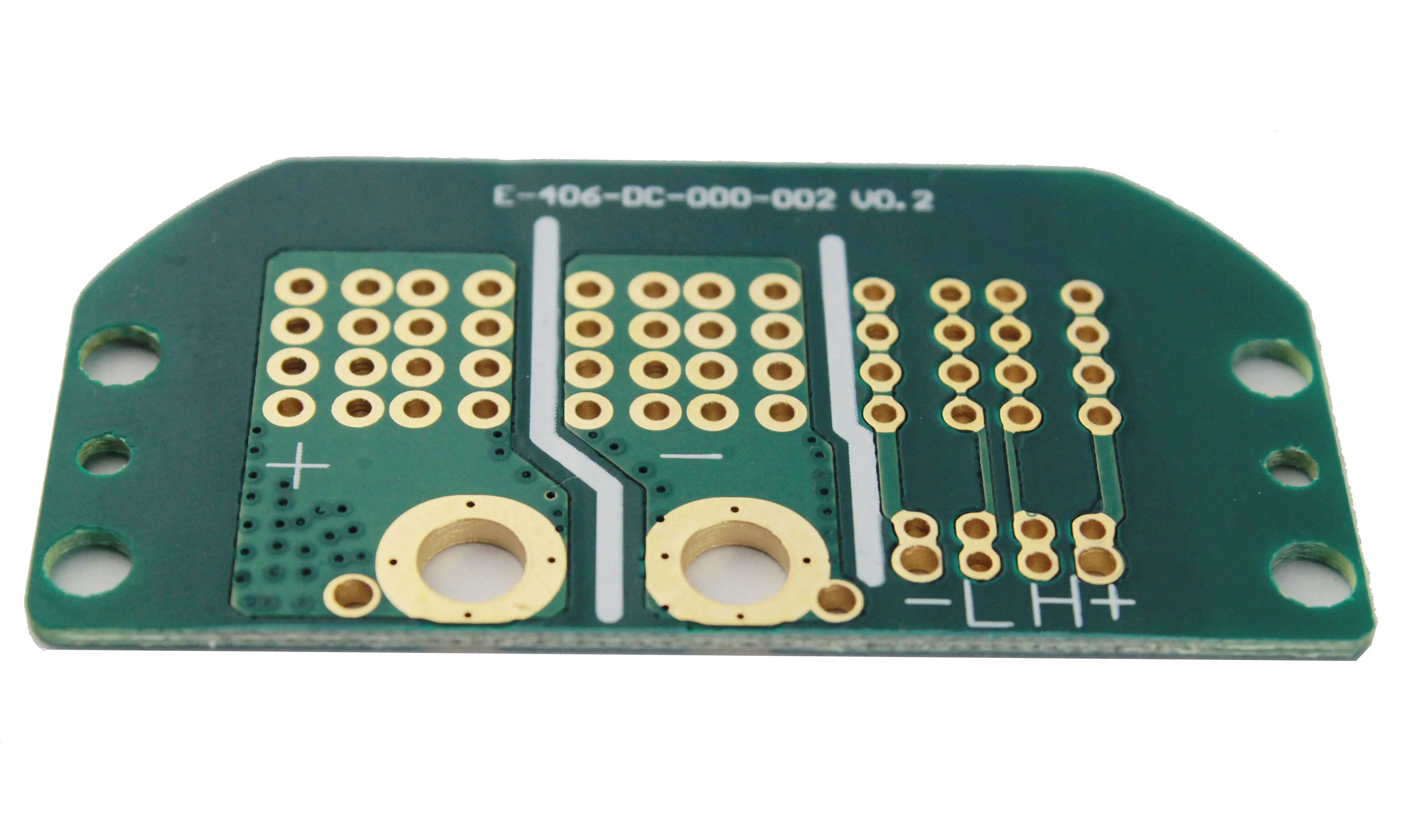
4. The line diameter is required, and the size of the embedded through hole is appropriate
The line that can be made wide shall never be made thin; High voltage and high frequency lines shall be round and smooth without sharp chamfers, and right angles shall not be used when turning. The ground wire should be as wide as possible, and it is better to use a large area of copper coating, which can greatly improve the docking point problem. The size of the pad or wire hole is too small, or the pad size and the drilling size are not matched properly. The former is disadvantageous to manual drilling, while the latter is disadvantageous to numerical control drilling. It is easy to drill the pad into "c" shape, or drill off the pad if it is heavy. The wire is too thin, and the large area of non wiring area is not set with copper coating, which is easy to cause uneven corrosion. That is, after the corrosion of the unrouted area, the thin wire is likely to be excessively corroded, or seEMIngly broken, or completely broken. Therefore, the function of copper coating is not only to increase the ground wire area and anti-interference.
5. Number of vias Solder joints and linear density
Some problems are not easy to be found in the early stage of circuit production, and they often emerge in the later stage. For example, there are too many wire holes, and a little carelessness in the copper sinking process will lead to hidden dangers. Therefore, wire holes shall be minimized in the design. The density of parallel lines in the same direction is too large, and it is easy to connect into one piece during welding. Therefore, the linear density shall be determined according to the level of welding process. The distance between welding points is too small, which is not conducive to manual welding. The welding quality can only be solved by reducing work efficiency. Otherwise, hidden dangers will be left. Therefore, quality and work efficiency of the welding personnel should be comprehensively considered when determining minimum distance of the welding spot.
If you can fully understand and master the above PCB design considerations, you can greatly improve the design efficiency and product quality. Correcting the existing errors during production will save a lot of time and cost, as well as rework time and material input.
PCB manufacturers, PCB designers and PCBA manufacturers will explain to you what is particularly important about the PCB design of power supply.


抖音二維碼

Q Q二維碼

微信二維碼
點擊
然后
聯(lián)系
然后
聯(lián)系
電話熱線
13410863085Q Q

微信

- 郵箱