鑫景福致力于滿足“快速服務,零缺陷,輔助研發”PCBA訂購單需求。


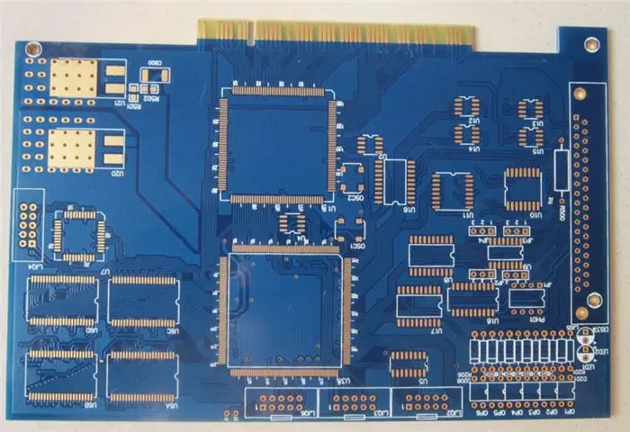
PCBA方案設計
Precautions on PCB electroplating line and knowLEDge to be mastered in wiring
PCB manufacturing, PCB design and PCBA processing manufacturers will explain to you the precautions for PCB electroplating line and the knowledge to be mastered for wiring
Today we mainly introduce the precautions of PCB electroplating line of PCB manufacturers. Have you paid attention to them?
1. Precautions for electroplating line, safety production and emergency handling:
(1) The copper bars of the auxiliary anode must be the same length as the production plate, about 5 cm wide, and arranged close to the plate.
(2) The auxiliary copper bar has become thICk and cannot be used again.
(3) The whole plate and pattern plated plate shall be made within 24 hours.
(4) The upper plate of the pattern plating shall wear SPInning gloves, the lower plate shall wear brown rubber gloves, the whole upper plate shall wear rubber gloves, and the lower plate shall wear dry roving gloves.
(5) Wear protective helmet, protective leather skirt and rubber gloves when adding nitric acid and sulfuric acid.
(6) When all materials are added, they need to be added when there is no plate in the cylinder. When copper sulfate, stannous sulfate and sodium persulfate are added, they need to be dissolved with water first, and then added to the central control tank of water (copper cylinder) or added to the plating tank when there is no plate in the cylinder.
(7) In case of driving failure and failure of normal production, the plates shall be removed in the following order: micro etching → degreasing → copper plating → tin plating → acid pickling. All plates are taken out of the rack after being washed in the corresponding water washing tank, and the cylinder number and electroplating time are MARKed.
(8) Stop production time: 2 hours requires 15 ASF to tow cylinders for 1 hour, and stop production time: 8 hours requires 10 ASF and 20 ASF to tow cylinders for 1 hour.
2. Precautions when resuming production
(1) The original copper cylinder was not plated with copper plate after the normal process pretreatment, and the normal follow-up work was proposed after the accumulated electroplating time reached 60 minutes.
(2) The original copper plated unplated tin plate is normally plated in the lower tin cylinder after normal pretreatment.
(3) The original lower tin plating cylinder plate 4 # was DIPped in acid and then tinned again until the accumulative time reached 10 minutes.
(4) The original pretreatment board is produced according to the normal process.
(5) In case of abnormality, the plate shall be plated and then submitted to the inspector for full inspection.
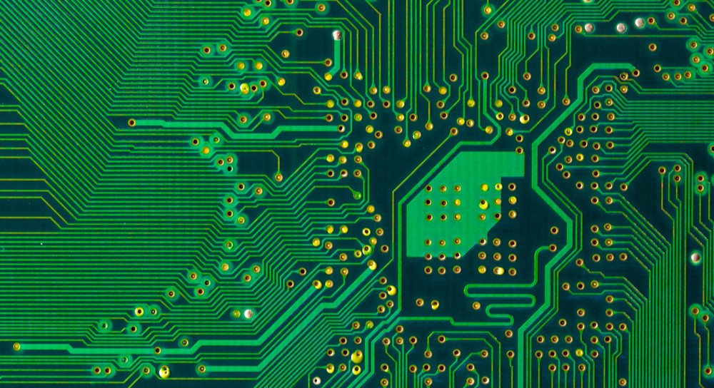
What knowledge is required for cabling?
PCB wiring is to lay printed wires according to PCB circuit schematic diagram, wire list and required wire width and spacing. So, what knowledge do you need to know about pcb board wiring?
1. On the prEMIse of meeting the requirements, the wiring shall be as SIMple as possible. The routing method is selected in the order of single-layer, double-layer and multi-layer.
2. Grounding wire shielding shall be arranged beside the input line of analog circuit; The wires in the same layer shall be evenly distributed; The conductive area of each layer shall be relatively balanced.
3. The signal line shall be inclined or smoothly transited when changing direction to avoid electric field concentration, signal reflection and additional impedance.
4. Digital circuit and analog circuit shall be separated in wiring to avoid mutual interference; The signal lines with different frequencies shall be separated by grounding wires to avoid crosstalk. In order to facilitate testing, necessary breakpoints and test points shall be set in the design.
5. The circuit components shall be grounded and connected to the power supply as short and close as possible to reduce the internal resistance.
6. The upper and lower layers of wiring shall be perpendicular to each other to reduce coupling, and the upper and lower layers of wiring shall not be aligned or parallel.
7. The length of multiple I/O lines of high-speed circuit, differential amplifier, balance amplifier and other circuits shall be equal to avoid unnecessary delay or phase shift.
8. When the pcb bonding pad is connected with a large conductive area, a thin wire with a length of not less than 0.5m shall be used for thermal isolation, and the width of the thin wire shall not be less than 0.13mm.
9. The wire closest to the edge of SMB shall be more than 5mm away from the edge of SMB, and the grounding wire can be close to the edge of SMB when necessary.
10. The common power cord and ground wire on the double-sided SMB should be laid near the edge of the SMB as far as possible and distributed on both sides of the SMB. Multi layer SMB can be equipped with power layer and ground wire layer in the inner layer, which are connected with power lines and ground wires of each layer through metallized holes. Large area wires, power lines and ground wires of the inner layer should be designed as a MESh.
PCB manufacturing, PCB design and PCBA processing manufacturers will explain to you the matters needing attention on PCB plating line and the knowledge to be mastered in wiring.


抖音二維碼

Q Q二維碼

微信二維碼
點擊
然后
聯系
然后
聯系
電話熱線
13410863085Q Q

微信

- 郵箱