鑫景福致力于滿足“快速服務,零缺陷,輔助研發”PCBA訂購單需求。


PCBA方案設計

Advantages of SMT packaging and PCB substrate materials
The advantages of SMT chip processing and packaging exceed the traditional packaging
1. ElectronIC equipment has SMAll volume and high installation density
The size of SMT chip electronIC components is only about 10% of the traditional package electronic components, and the quality is only 10% of the traditional plug-in electronic components. Surface Mount Technology can generally reduce the size of electronic equipment by 40% - 60%, the quality by 60% - 80%, and greatly reduce the area and quality. The grid for processing and installing electronic components on SMT wafers has grown from 1.27 mm to 0.63 mm, and some have reached 0.5 mm. Through hole installation technology can improve the relative density of installation.
2. High reliability and strong anti vibration capability
SMT chip processing uses chip components with high reliability, small size, light texture, strong vibration resistance, automatic production, high installation reliability, and the ratio of defective solder joints is usually less than 10 parts per million The wave soldering technology of through hole plug-in electronic components should be one order of magnitude lower to ensure low defect rate of electronic equipment or component solder joints So far, nearly 90% of Electronic devices use surface mount technology
3. Good high-frequency characteristics and reliable performance Because the chip components are firmly instalLED, and the devices are usually lead-free or short leads, this reduces the impact of parasitic inductance and capacitance, improves the high-frequency characteristics of the circuit, and reduces electromagnetic and radio frequency interference. The maximum frequency of the circuit designed with SMC and SMD can reach 3 GHz, while the chip electronic components are only 500 MHz, which can shorten the transmission delay time. It can be used in circuits with clock frequency higher than 16MHz. If MCM technology is selected, the high-end clock frequency of the computer workstation can reach 100 MHz, and the additional power consumption caused by parasitic reactance can be greatly reduced by 2-3 tiMES.
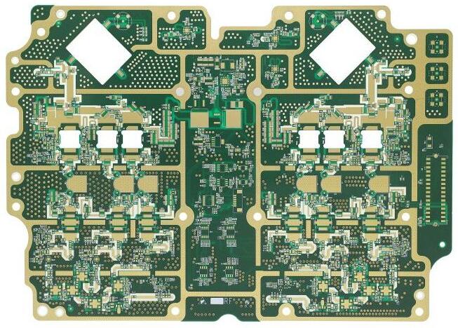
Printed circuit board

4. Improve production efficiency and realize automatic production
Up to now, in order to realize the complete automation of perforated installation of printed circuit boards, it is necessary to expand the area of the original printed circuit board by 40%, so that the insertion head of the automatIC parts can be inserted into the electronic components. Otherwise, insufficient clearance and parts damage will occur. The automatic placement machine (SM421/SM411) uses a vacuum nozzle to suck and discharge electronic components. The shape of the vacuum nozzle is smaller than that of the electronic components, which increases the relative density of the installation. In fact, small electronic components and fine pitch QFP devices are all produced by automatic mounters to achieve automatic production of the whole line.
5. Reduce costs and expenses
(1) The use area of PCB is reduced, which is 1/12 of that of through-hole technology. If CSP installation is selected, the area will be greatly reduced;
(2) Reduce the number of holes in the printed circuit board, greatly saving the rework cost;
(3) Due to the improvement of frequency characteristics, the cost of circuit debugging is greatly reduced;
(4) Due to the small size and light texture of the chip module, the packaging, transportation and storage costs are greatly reduced;
SMT processing technology can greatly save data, energy, equipment, manpower, time, etc. Costs can be significantly reduced by 30% and 50%.
classification of PCB PCB substrate data
In short, the base plate is the basic data for the production of PCB. Generally speaking, PCB substrate consists of resin, reinforcement materials and conductive materials, and there are many types. The most common resins are epoxy and phenolic. The enhancement materials include paper base, glass cloth, etc. The most commonly used conductive material is copper foil. Copper foil is divided into electrolytic copper foil and rolled copper foil.
PCB subset material classification:
1. According to different reinforcement data:
1. Paper substrate (FR-1, FR-2, FR-3);
2. Epoxy glass fiber cloth substrate (FR-4, FR-5);
3. Composite substrate (CEM-1, CEM-3 (composite epoxy material grade 3);
4. HDI (High Density Interconnection) PCB (RCC);
Special substrate (metal substrate, ceramic substrate, thermoplastic substrate, etc.).
2. According to flame retardancy:
1. Flame retardant (UL94-V0, UL94V1);
2. Non flame retardant (UL94-HB grade).
3. Depending on the resin:
1. Phenolic resin PCB board;
2. Epoxy resin PCB board;
3. Polyester resin PCB board;
4. BT resin PCB board;
5. PI resin pcb board.


抖音二維碼

Q Q二維碼

微信二維碼
點擊
然后
聯系
然后
聯系
電話熱線
13410863085Q Q

微信

- 郵箱