鑫景福致力于滿足“快速服務,零缺陷,輔助研發(fā)”PCBA訂購單需求。


PCBA方案設計

PCB proofing and PCB processing etching process
Make sure the signal line is as short as possible for PCB proofing
When the length of signal line is greater than 300mm, the grounding wire must be laid in parallel
Ensure that the loop area between the signal line and the corresponding loop is as SMAll as possible For long signal lines, the positions of signal lines and ground wires must be switched every few centimeters to reduce the loop area
Drive signals from the network center into multiple receiving circuits
Ensure that the loop area between the power supply and the grounding is as small as possible, and place high-frequency capacitors near each power pin of the integrated circuit chip
Place a high-frequency bypass capacitor within 80mm of each connector
If possible, fill unused areas with land and connect each layer of fill every 60mm
Ensure that this two alternative end positions of an extremely large ground filling area (approximately greater than 25mm * 6mm) are connected to the ground
When the length of the opening on the power supply or ground plane exceeds 8 mm, use a narrow wire to connect both sides of the opening
The reset line, interrupt signal line or edge trigger signal line cannot be arranged near the edge of PCB
Connect the mounting holes to the circuit common ground, or isolate them
(1) When the metal bracket must be used with a metal shielding devICe or a chassis, a zero ohm resistance shall be used for connection
(2) Determine the size of the mounting hole to achieve reliable installation of metal or plastic brackets. Use large pads on the top and bottom layers of the mounting holes, and do not use solder resist on the bottom pad, and ensure that the bottom pad does not use wave soldering technology Welding
The protected signal line and unprotected signal line cannot be arranged in parallel
PCB proofing shall pay special attention to reset wiring, interrupt and control signal line
(1) High frequency filtering should be used.
(2) Keep away from input and output circuits.
(3) Keep away from the edge of the PCB
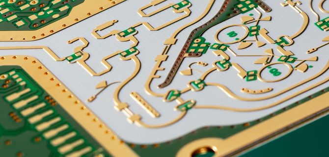
PCB board

This PCB proofing should be inserted into the main housing, not instalLED in the opening position or the inner seam
Note the wiring below the magnetic bead, between the pad and the signal wire that may contact the magnetic bead Some magnetic beads have good conductivity, which may lead to unexpected conductive paths
If there are several PCB boards in a chassis or motherboard, the PCB board most sensitive to static electricity should be placed in the middle
The etching state of the leading edge and the training edge are different
A lot of problems related to etching quality are concentrated on the etched part of the upper plate surface. It is very important to understand this These problems are due to the influence of colloidal lumps produced by etchants on the surface of printed circuit boards On the one hand, the colloidal stone plate with a large copper surface area will affect the spraying force; on the other hand, it will prevent the supplement of fresh etching solution, which will reduce the etching speed It is due to the formation and accumulation of colloidal boards that the upper and lower patterns of circuit boards are etched to different degrees This also makes the first part of the circuit board in the etching machine easy to be completely etched or lead to excessive corrosion, because there is no accumulation at that time, and the etching speed is faster On the contrary, the part after entering the plate has formed when entering and slows down its etching speed
Maintain PCB etching equipment
The most critical factor in maintaining the etching equipment is to ensure that the nozzle is clean and free of obstacles so that the jet can flow freely Under the action of jet pressure, blockage or slagging will affect the layout If the nozzle is not clean, this will cause uneven etching and discard the entire PCB
Obviously, equipment maintenance is to replace damaged and worn parts, including nozzle replacement The nozzle also has wear problems In addition, the more critical problem is to keep the etcher free of slagging In many cases, there will be slagging accumulation Excessive slagging may even affect the chEMIcal balance of the etching solution SIMilarly, if there is excessive chemical imbalance in the etching solution, slagging will become more serious The problem of slag accumulation cannot be overemphasized Once a large amount of slagging suddenly appears in the etching solution, this is usually a signal indicating that there is a problem with the balance of the solution Strong hydrochloric acid shall be used for cleaning or replenishing the solution


抖音二維碼

Q Q二維碼

微信二維碼
點擊
然后
聯(lián)系
然后
聯(lián)系
電話熱線
13410863085Q Q

微信

- 郵箱