鑫景福致力于滿足“快速服務,零缺陷,輔助研發”PCBA訂購單需求。


PCBA方案設計

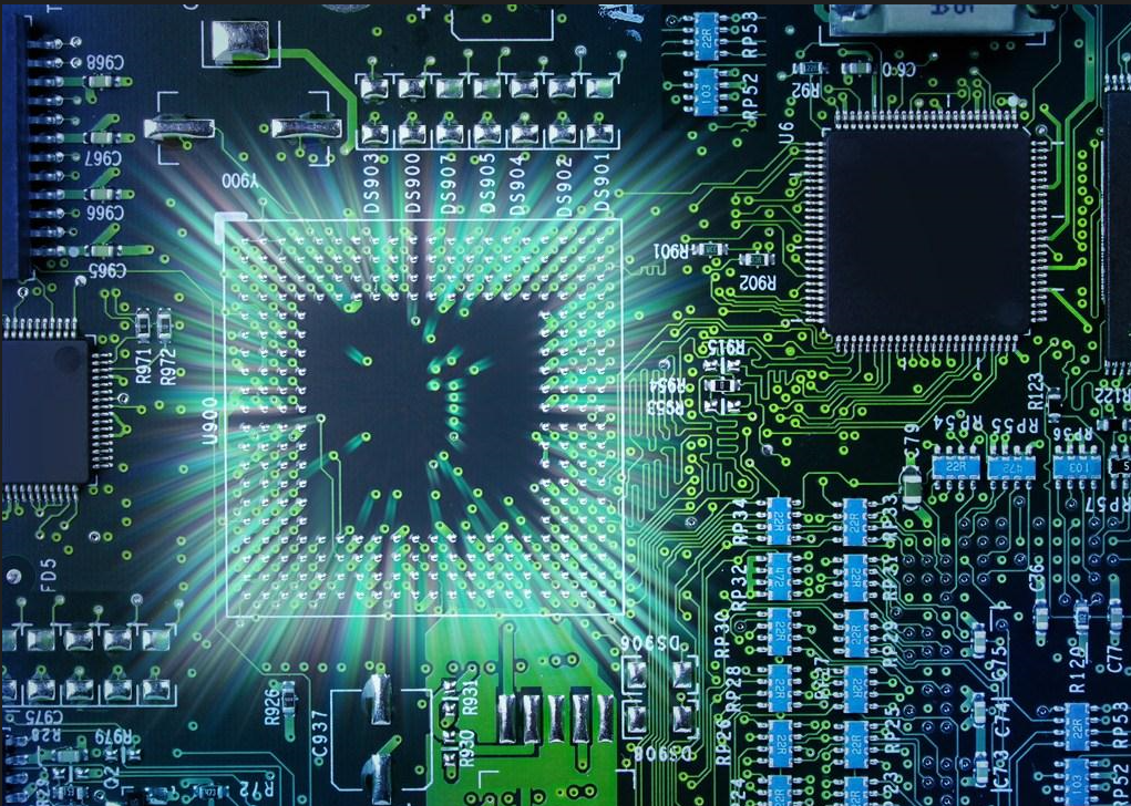
Etching Process Control Method in PCB Processing
Type 1 PCB Etching
It should be noted that during the etching process, there are two layers of copper on the circuit board In the outer etching process, only one layer of copper must be completely etched, and the rest will form the final required circuit The feature of this pattern electroplating is that the copper plating layer only exists below the lead tin resistance layer Another process is to plate copper on the whole circuit board, and the part outside the photosensitive film is only tin or lead tin resist This process is calLED "full plate copper plating process" Compared with pattern electroplating, the biggest disadvantage of copper plating on the entire circuit board is that all parts of the circuit board must be copper plated twICe, and all parts must be corroded during the etching process Therefore, when the wire width is very thin, a series of problems will occur At the same time, side corrosion will seriously affect the uniformity of the circuit
PCB Etching

Another method is to deal with printed circuit boards of external circuits of science and technology, that is, to use photosensitive films instead of metal coatings as corrosion resistant layers This method is very SIMilar to the inner layer etching process. You can refer to the etching in the inner layer manufacturing process At present, tin or lead tin is the most commonly used anti-corrosion coating for the etching process of amino etchant Amino etchant is a common chEMIcal liquid, which has no chemical reaction with tin or lead tin Ammonia etchant mainly refers to ammonia/ammonium chloride etching solution In addition, ammonium sulfate etching chemicals are also available on the ammonia/MARKet After using sulfate etching solution, the copper in it can be separated by electrolysis and reused Because of its low corrosion rate, it is usually rare in practical production, but it is expected to be used for chlorine free etching Someone tried to use hydrogen sulfate as an etchant to etch the outer pattern For many reasons, including economy and waste liquid treatment, this process has not been widely used commercially In addition, sulfuric acid hydrogen peroxide cannot be used for the etching of lead tin resist, and this process is not the main method for external production of PCB, so most people pay little attention to it
2. Etching quality of printed circuit board
The basic requirement for etching quality is to completely remove all copper layers except under the resist layer Strictly speaking, if accurate definition is required, then the etching quality must include the consistency of wire width and undercut degree Due to the inherent characteristics of the current etching solution, this will produce etching effects not only in the downward direction, but also in the left and right directions. Side etching is almost inevitable
Side etching is one of the most frequently discussed etching parameters It is defined as the ratio of side etching width to etching depth, which is called etching factor In the printed circuit industry, it has a wide range of changes, from 1:1 to 1:5. Obviously, SMAller undercut or lower etching coefficient is the most satisfactory
The structure of etching equipment and etching solutions with different components will affect the etching factor or the extent of side etching, or optimistically, it can be controlled The use of certain additives can reduce the degree of side erosion The chemical composition of these additives is usually a trade secret, and their respective developers have not disclosed it to the public In many ways, etching quality exists long before the printed board enters the etching machine Because each process of printed circuit processing has a very close internal relationship, there is no process that is not affected by other processes and does not affect other processes Many problems identified as etching quality actually exist in the process of removing films, even before It is used for the etching process of the outer layer graphics. Because the "countercurrent" phenomenon it represents is more prominent than most PCB processes, many problems are finally reflected in it At the same time, this is also because etching is the last step in a series of processes starting from self adhesion and photosensitivity, after which the outer pattern is successfully transferred The more links, the greater the possibility of problems This can be regarded as a very special aspect of the printed circuit production process
Theoretically, after the printed circuit enters the etching stage, in the process of processing the printed circuit through pattern electroplating, the ideal state should be: after electroplating, the total thickness of copper and tin or copper and lead tin should not exceed the thickness of the electroplating resistance photosensitive film, so that the electroplating pattern is completely blocked by the "walls" on both sides of the film and embedded in it However, in actual production, the electroplating pattern is much thicker than the photosensitive pattern around the world In the process of electroplating copper and lead tin, because the electroplating height is higher than the photosensitive film, there is a trend of horizontal accumulation, which leads to the problem The tin or lead tin anti-corrosive layer covering the line extends to both sides to form an "edge", under which a small part of the photosensitive film is covered
The "edge" formed by tin or lead tin makes it impossible to completely remove the film when removing it, leaving a small part of "residual glue" under the "edge" The "residual glue" or "residual film" left under the "edge" of the resist will lead to incomplete etching After etching, the lines form "copper root" on both sides The copper root reduces the line spacing, resulting in the printed board not meeting the requirements of Party A, and may even be rejected Rejection will greatly increase the number of printed circuit boards
In addition, in many cases, due to the formation and dissolution of reaction, in the printed circuit industry, residual films and copper may also form and accumulate in corrosive liquids, and block the nozzles of corrosion machines and acid resistant pumps. It must be closed for treatment and cleaning, Affect work efficiency
The above is the explanation given by the editor of pcb circuit board company.
If you want to know more about PCBA, you can go to our company's home page to learn about it.
In addition, our company also sells various circuit boards,
High Frequency Circuit Board and SMT chip are waiting for your presence again.


抖音二維碼

Q Q二維碼

微信二維碼
點擊
然后
聯系
然后
聯系
電話熱線
13410863085Q Q

微信

- 郵箱