鑫景福致力于滿足“快速服務(wù),零缺陷,輔助研發(fā)”PCBA訂購(gòu)單需求。


PCBA方案設(shè)計(jì)

Overview of hedging methods for four layer PCB
Four layer quality PCB is defined in IPC The surface treatment is oxidation resistant If the vacuum package is not opened and used within half a year, the vacuum package will be removed within 24 hours to control the temperature and humidity It shall be used within one year in the environment without opening the packaging of the circuit board After opening, it should be pasted within one week and one hour Temperature and humidity must also be controlLED Gold plate is equivalent to tin plate, but the control process is strICter than tin plate
Generally speaking, the four layer circuit board can be divided into the top layer, the bottom layer and two intermediate layers. The top and bottom layers are wired with signal cables. In the middle layer, first use the command design/Layer Stack Manager to add INTERNAL PLANE1 and INTERNAL PLANE2, where add PLANE is the most commonly used PCB power layer, such as VCC and ground plane, such as GND (that is, connect the corresponding network label. Be careful not to use add layer, which will add MIDPLAYER, which is mainly used for signal wire placement of multilayer PCB). In this case, PLNNE1 and PLANE2 are two layers of copper wire connecting power supply VCC and ground GND.
Four layer PCB refers to a printed circuit board made of four layers of glass fiber Generally, SDRAM uses four layers of boards Although this will increase the cost of PCB, noise interference can be avoided
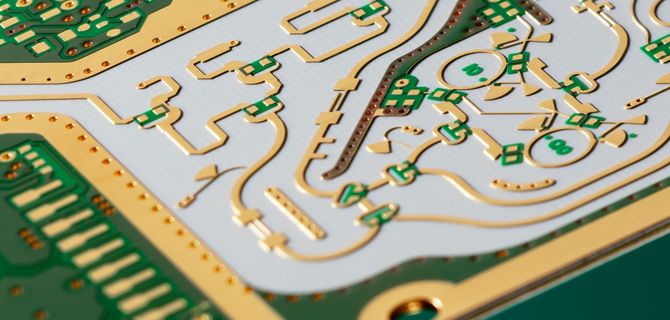
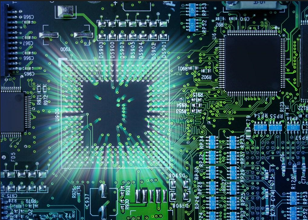
Circuit board

General principles for the layout and wiring of multilayer PCB circuit boards The general principles that PCB designers need to follow in the wiring process of circuit boards are as follows:
(1) Set the principle for printing trace spacing of components. The spacing constraint between different networks is based on the principle of setting component printing trace spacing through electrical insulation, manufacturing technology and components. It is determined by size and other factors. For example, if the pin spacing of the chip component is 8mil, the [ClearanceConstraint] of the chip cannot be set to 10mil. PCB designers need to set 6mil PCB design rules separately for chips. At the same time, the spacing setting should also consider the manufacturer's production capacity.
In addition, an important factor affecting components is electrical insulation. If the potential difference between two components or networks is large, electrical insulation needs to be considered. The clearance safety voltage under general environment is 200V/mm, i.e. 5.08V/mil. In this case, when there are high-voltage and low-voltage circuits on the same circuit board, it is necessary to pay special attention to sufficient safety clearance. When there are high voltage circuits and low voltage circuits, it is necessary to pay special attention to sufficient safety distance.
(2) Selection of wiring form at the line corner. In order to make the circuit board easy to manufacture and beautiful, it is necessary to set the circuit corner mode and the selection of circuit corner wiring form when designing PCB. 45 °, 90 ° and radian can be selected. In general, acute angles are not used. It is better to use arc transition or 45 ° transition, and avoid transition with 90 ° or more acute angles.
The connection between the conductor and the gasket should also be as smooth as possible to avoid SMAll sharp feet, which can be solved through tears. When the center distance between pads is less than the outer diameter D of pads, the width of wire can be the same as the diameter of pads; If the center distance between pads is greater than D, the width of the wire should not be greater than the width of the pad diameter. When the wire passes between two pads but is not connected with them, the maximum and equal distance shall be kept from them. SIMilarly, when a wire and one of the wires pass through two pads without connecting with them, the maximum and equal spacing shall be maintained, and the spacing between them shall also be uniform, equal and maximum. The spacing between them should also be uniform and equal, and kept the maximum.
(3) How to determine the width of the print trace. The width of the track is determined by such factors as the current level flowing through the conductor and anti-interference. The greater the overcurrent flowing through the current, the wider the track should be. The power line shall be wider than the signal line. In order to ensure the stability of the ground potential (the greater the change of the ground current, the wider the track should be. Generally, the power line should be wider than the signal line, and the influence of the power line should be smaller than the signal line width), and the ground wire should also be longer. The wide ground wire should also be wider. The experiment proves that when the copper film thickness of the printed wire is 0.05mm, the current carrying ground wire of the printed wire should also be wider and can be calculated as 20A/mm2, that is, the wire with 0.05mm thickness and 1mm width can flow 1A current. In general, the general width can meet the requirements; For high voltage and high voltage, the width of signal line is 10-30 mils, which can meet the requirements of high voltage and high current signal lines with line width greater than or equal to 40 mils and line spacing greater than 30 mil. In order to ensure the anti stripping strength and working reliability of the conductor, the conductor shall be as wide as possible to reduce the line impedance and improve the anti-interference efficiency within the allowable range of board area and density.
For the width of the power line and ground wire, in order to ensure the stability of the waveform, if the wiring space of the circuit board allows, thicken it as much as possible. Generally, it requires at least 50mil.
(4) Anti-interference and electromagnetic shielding of PCB printed wires. The interference introduced by the power line) the anti interference and electromagnetic shielding of the printed wires Interference on wires mainly includes interference introduced between wires, crosstalk between PCB signal lines, and crosstalk between signal lines Reasonable wiring and grounding pipe layout can effectively reduce interference sources and make PCB design PCB have better electromagnetic compatibility


抖音二維碼

Q Q二維碼

微信二維碼
點(diǎn)擊
然后
聯(lián)系
然后
聯(lián)系
電話熱線
13410863085Q Q

微信

- 郵箱