鑫景福致力于滿足“快速服務(wù),零缺陷,輔助研發(fā)”PCBA訂購單需求。


PCBA方案設(shè)計(jì)
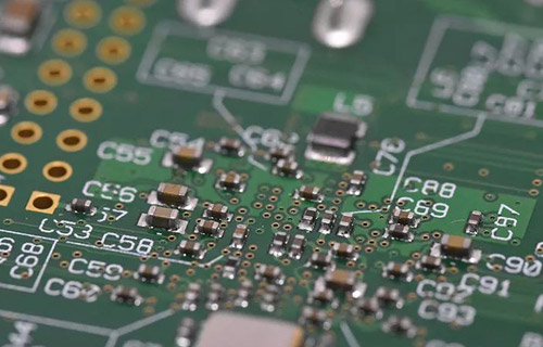
Different processes of pads on circuit boards
The following describes the impact of different processes on pads on PCB:
1 If the PCB chip assembly is not connected to the PCB component, a test point must be added The diameter of the test point should be between 1. 0 mm and 1.5 mm, whICh is convenient for online testing The edge of the test point pad shall be at least 0. 4mm away from the surrounding pad edge The diameter of the test pad is greater than 1mm and must have network characteristics The center distance between two test pads shall be greater than or equal to 2.54mm; If the through-hole is used as a measuring point, a pad must be added outside the through-hole The diameter Above 1mm (inclusive);
2. PCB pad must be added at the position of the hole with power connection; All pads must have network content. Network naMES cannot be the same for networks without connected components; The distance between the center of the positioning hole and the center of the test pad is greater than 3mm; Other irregular shapes, but with power connection slots, pads, etc., are evenly placed on mechanical layer 1 (referring to single insert, fuse and other slots).
3. If the pin pad of components with dense pin spacing (pin spacing less than 2.0mm) (such as IC, swing socket, etc.) is not connected to the pad of manual parts, a test pad must be added. The diameter of the test point shall be between 1.2mm and 1.5mm, so that it can be tested by the on-line tester.
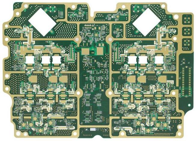
Circuit board

4. If the distance between pads is less than 0.4mm and exceeds the wave crest, white oil must be applied to reduce continuous welding.
5. The tip and end of the patch assembly in the gluing process shall be designed as lead tin. It is recommended to use 0.5mm conductor for the width of lead and tin, and the length is generally 2 or 3mm.
6. If there are manually welded parts on the veneer, the tin bath should be removed in the opposite direction to the tin passing direction, and the hole width is 0.3mm to 0.8mm
7. The spacing and size of conductive rubber buttons shall be consistent with the actual size of conductive rubber buttons. The PCB connected with this shall be designed as a gold finger, and the corresponding gold plating thickness shall be specified (usually greater than 0.05um~0.015um).
8. The size and spacing of PCB pads shall match the size of SMD components
A. When there are no special requirements, the shapes of part holes, pads and part feet must match, and the symmetry of pads relative to the hole center shall be ensured (part holes and square pads in the form of square part feet; round part feet are equipped with round part holes and circular pads). Adjacent pads are independent of each other to prevent thin tin and wire drawing;
b. Adjacent component pins in the same circuit or compatible equipment with different pin spacing must have separate pad holes, especially compatible pads that encapsulate compatible relays. For example, you cannot set the PCB layout separately. The pad holes of the two pads must be surrounded by a solder mask
9. When designing multilayer boards, attention should be paid to the components of the metal housing. The housing and printed board are in contact with the printed board during insertion. The mat on the top layer cannot be opened and must be covered with green oil or screen oil.
10. In the process of PCB design and layout, try to reduce the slotting and opening of PCB to avoid affecting the strength of PCB
11. Valuable parts: Do not place valuable parts in the corners, edges, mounting holes, slots, notches and corners of the PCB. These locations are high stress areas of the printed board and may lead to soldering. Cracks and cracks in points and components.
12. Heavy components (such as transformers) shall not be far away from the positioning holes to avoid affecting the strength and deformation of printed boards. During layout, you should choose to place the heavier components under the PCB (and the last component to enter the wave soldering side).
13. Transformers, relays and other devices and circuits that can radiate energy shall be far away from amplifiers, single chip computers, crystal oscillators, reset circuits and other devices and circuits that are vulnerable to interference, so as not to affect the reliability of work.
14. QFP packaged integrated circuits (requiring wave soldering process) must be placed at 45 degrees, and pads should be added.


抖音二維碼

Q Q二維碼

微信二維碼
點(diǎn)擊
然后
聯(lián)系
然后
聯(lián)系
電話熱線
13410863085Q Q

微信

- 郵箱