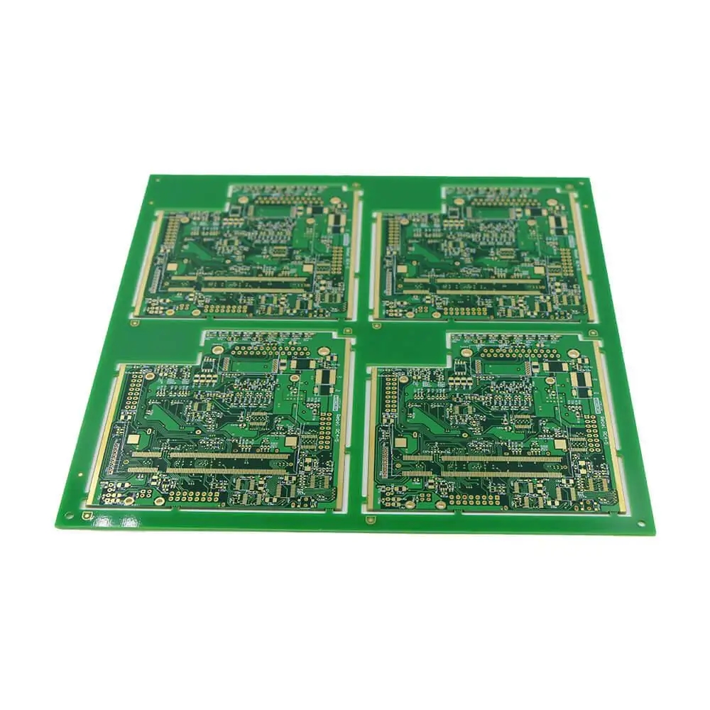
鑫景福致力于滿足“快速服務,零缺陷,輔助研發”PCBA訂購單需求。


PCBA方案設計
Listen to the old engineer explain PCB layout experience
PCB manufacturing, PCB design and PCBA processing manufacturers will explain to you the PCB layout experience of veteran engineers
For electronIC products, PCB design is a necessary design process from electrical schematic diagram to a specific product, and the rationality of its design is closely related to product production and product quality.
For many people who are just engaged in electronIC design, they have little experience in this field. Although they have learned the PCB design software, the PCB they have designed often has problems of one kind or another, and there are few articles on this aspect in many electronic journals. The author of this article has been engaged in PCB design for many years. Here, I would like to share my experience in PCB design with you, I hope it can play a role in attracting jade.
Layout of boards:
The normal order for placing components on PCB:
Place components in fixed positions closely matching with the structure, such as power sockets, indicator lights, switches, connectors, etc. After placing these components, lock them with the LOCK function of the software, so that they will not be moved by mistake in the future;
Place special components and large components on the circuit, such as heating components, transformers, ICs, etc;
Place the widget. Distance from components to the edge of the board: if possible, all components should be placed within 3mm from the edge of the board or at least greater than the thickness of the board. This is because it should be provided for the use of the guide rail slot during mass production of assembly line plug-ins and wave soldering. At the same time, in order to prevent edge defects caused by external processing, if there are too many components on the printed circuit board, they must not exceed the 3mm range, A 3mm auxiliary edge can be added to the edge of the plate. The auxiliary edge can be broken with a V-shaped groove during production.
Isolation between high voltage and low voltage: There are high voltage circuits and low voltage circuits on many PCB at the same time. The components of the high voltage circuit should be separated from the low voltage part. The isolation distance is related to the withstand voltage to be borne. Generally, the distance on the board is 2mm at 2000kV, which should be increased by comparison. For example, if the withstand voltage test of 3000V is to be borne, the distance between the high voltage and low voltage lines should be more than 3.5mm, In many cases, to avoid creepage, slots are also made between high and low voltage on the printed circuit board.
PCB routing:
The layout of printed wires shall be as short as possible, especially in high-frequency circuits; The corners of printed wires should be rounded, and right angles or sharp corners will affect the electrical performance in the case of high frequency circuits and high wiring density; When wiring the two panels, the conductors on both sides should be perpendicular, oblique, or bent to avoid parallel, so as to reduce parasitic coupling; The printed wires used as the input and output of the circuit shall not be adjacent and parallel as much as possible to avoid feedback. It is better to add grounding wires between these wires.
Width of printed wire:
The wire width should meet the electrical performance requirements and be convenient for production. Its SMAller value depends on the current it bears, but the smaller value should not be less than 0.2mm. In high-density and high-precision printed circuits, the wire width and spacing can generally be 0.3mm; The temperature rise of the conductor width should also be considered under the condition of large current. The single panel experiment shows that when the copper foil thickness is 50 μ m. When the conductor is 1~1.5mm wide and the current is 2A, the temperature rise is very small. Therefore, the conductor with a width of 1~1.5mm may meet the design requirements without causing temperature rise.
The common ground wire of the printed wire should be as thick as possible. If possible, use lines larger than 2-3 mm, which is particularly important in the circuit with a microprocessor. Because when the local wire is too thin, the noise tolerance will be degraded due to the change of the current flowing, the change of the ground potential, and the unstable level of the microprocessor timing signal; The principles of 10-10 and 12-12 can be applied to routing between IC pins of DIP package, that is, when two pins pass through two wires, the pad diameter can be set to 50mil, and the line width and line spacing can be set to 10mil; when only one wire passes between two pins, the pad diameter can be set to 64mil, and the line width and line spacing can be set to 12mil.
Spacing of printed wires:
The spacing between adjacent conductors must meet the electrical safety requirements, and in order to facilitate operation and production, the spacing should also be as wide as possible. The small spacing shall at least be suitable for the withstand voltage. This voltage generally includes working voltage, additional fluctuating voltage and peak voltage caused by other reasons. If the relevant technical conditions allow a certain degree of metal residues between conductors, their spacing will be reduced. Therefore, the designer should take this factor into account when considering the voltage. When the wiring density is low, the spacing of signal lines can be appropriately increased, and the signal lines with high and low level differences should be as short as possible and the spacing should be increased.
Shielding and grounding of printed wire:
The common ground wire of the printed wire shall be arranged at the edge of the printed circuit board as far as possible. Copper foil should be reserved as much as possible on the PCB as ground wire, so that the shielding effect is better than a long ground wire. The transmission line characteristics and shielding effect will be improved, and the distributed capacitance will be reduced.
The common ground wire of the printed wire is better to form a loop or network. This is because when there are many integrated circuits on the same board, especially the components that consume more power, the ground potential difference is generated due to the restrictions on the graphics, thus reducing the noise tolerance. When the circuit is made, the ground potential difference is reduced.
In addition, the figure of grounding and power supply should be parallel to the flow direction of data as much as possible, which is the secret of enhancing the ability to suppress noise; Several layers of multilayer PCB can be used as shielding layers. Power supply layer and ground wire layer can be regarded as shielding layers. Generally, ground wire layer and power supply layer are designed in the inner layer of multilayer PCB, and signal wire is designed in the inner layer and outer layer. PCB manufacturers, PCB designers and PCBA manufacturers will explain their PCB layout experience to you.


抖音二維碼

Q Q二維碼

微信二維碼
點擊
然后
聯系
然后
聯系
電話熱線
13410863085Q Q

微信

- 郵箱