鑫景福致力于滿足“快速服務,零缺陷,輔助研發”PCBA訂購單需求。


PCBA方案設計

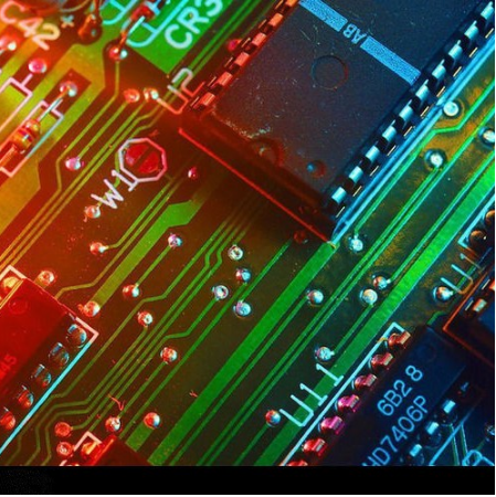
The role played by PCB is to provide a base for connecting the components that complete the first level of construction with other necessary electronIC parts to form a module or finished product with specifIC functions. Therefore, PCB plays the role of integrating all functions of the connecting assembly in the entire electronic product. Therefore, PCB is often the first to be questioned when electronic product function fails.
Evolution of PCB 1. Earlier than 1903, Mr Albert Hanson pioneered the use of the "Circuit" concept in the telephone exchange system. It is cut into circuit conductors with metal foil, stuck to paraffin paper, and also pasted with a layer of paraffin paper, which has become the prototype of modern PCB mechanism. By 1936, Dr Paul Eisner had truly invented the PCB manufacturing technology and also published several patents. And today's print etch (photo image transfer) technology is based on its invention.
The variety of PCB types and manufacturing methods in terms of materials, levels and processes is suitable for different electronic products and their special needs.
PCB
PCB double-sided board
Cutting, drilling, copper sinking, plate surface electroplating, pattern transfer, electroplating, etching quality inspection, printing solder mask oil (green oil/white words), gold sinking, tin spraying, gold plating, V-CUT gongs, beer room test, FQC packaging, finished product warehouse delivery
PCB multilayer board
Cutting inner layer DF AOI browning pressing plate drilling room copper sinking plate surface electroplating outer layer DF outer layer etching QC11 green oil, white word gold sinking, tin spraying, gold plating V-CUT gongs room, beer room testing FQC packaging finished products warehouse shipment
PCB copper surface treatment (grinding brush)
Printing ink (different screen inks have different MEShes, generally 77T or 57T)
Pre baking (different ink parameters, generally 75-80 degrees)
Exposure (exposure energy level 10-12)
Development (55% of development point)
Visual inspection -
Post curing (150 ° C for 60 minutes)
PCB production process can be divided into several aspects, including single panel process, double-sided process, and multi-layer process. In addition to general hard boards, soft boards are also flexible boards FPC, and there are also several processes, namely single-layer FPC, multi-layer FPC, etc
Layout principles in high-speed PCB design
In the process, special components refer to the key components of the high-frequency part, the core components of the circuit, the PCB components that are vulnerable to interference, the high-voltage components, the components with high heat, and some components. For heterosexual components, the positions of these special components need to be carefully analyzed to make the layout meet the requirements of circuit functions and requirements. Incorrect placement of them will cause circuit compatibility problems, signal integrity problems, and lead to PCB design failure.
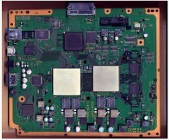
Pcb design
When considering the placement of special components in PCB design, first consider the PCB size. When the PCB size is too large, the printing line is long, the impedance increases, the drying resistance decreases, and the cost increases; When it is too SMAll, the heat dissipation is poor, and adjacent lines are easily disturbed. After determining the size of PCB during PCB design, determine the position of special components. Finally, all components are laid out according to functional units. When arranging, the location of special components usually follows the following principles:
1. The pcb is designed to shorten the connection between high-frequency components as much as possible, and reduce their distribution parameters and mutual electromagnetic interference as much as possible. Elements susceptible to interference shall not be too close, and the input and output shall be as far away as possible.
2 Some components or wires may have high potential difference, and their distance shall be increased to avoid accidental short circuit caused by discharge. High voltage components shall be placed in places that cannot be touched by hands.
3. Components weighing more than 15G can be fixed with brackets and then welded. Those heavy and hot components should not be placed on the circuit board, but on the backplane of the main frame, and heat dissipation should be considered. The thermal element shall be kept away from the thermal element.
4. For the layout of adjustable elements, such as potentiometers, adjustable inductors, variable capacitors, microswitches, etc., the structural requirements of the whole wrench shall be considered. When the structure allows, some common switches shall be used. Put it in an easily accessible place. The Layout of components is balanced, the density is dense, and it is not top heavy.
The success of the product lies in its focus on internal quality. The second is to consider the overall aesthetics, both of which are more perfect boards and become a successful product. The quality is mainly attributed to the PCB production materials and PCB manufacturing process. The overall aesthetics must depend on the aesthetics of schematIC design of PCB design engineers.


抖音二維碼

Q Q二維碼

微信二維碼
點擊
然后
聯系
然后
聯系
電話熱線
13410863085Q Q

微信

- 郵箱