鑫景福致力于滿足“快速服務,零缺陷,輔助研發”PCBA訂購單需求。


PCBA方案設計
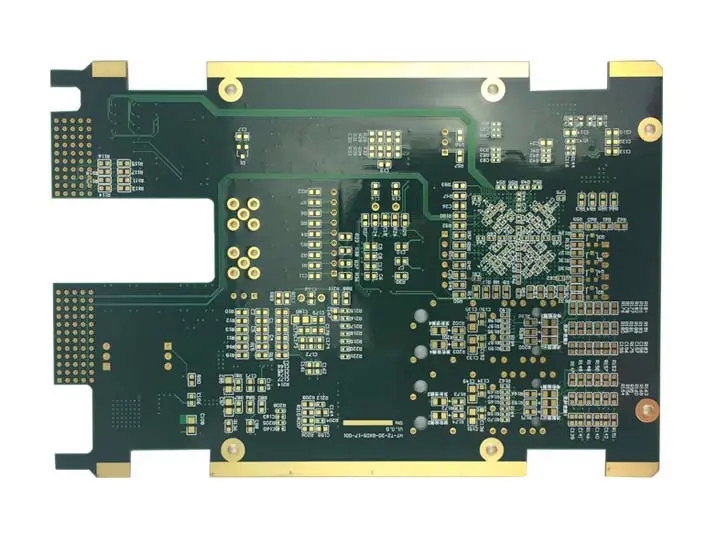
Introduction to PCB design from Shallow to Deep
circuit board manufacturing, circuit board design and PCBA processing manufacturers explain to you
When I saw the PCB of the computer motherboard, I thought it would be great to draw it myself. Later, when I CAMe into contact with protel99se, I stepped into the team of drawing boards, and then altium, CADence, etc. With the accumulation of experience in drawing boards, more and more matters need attention. A good PCB does not just connect the wires. Let me talk about the story in it slowly.
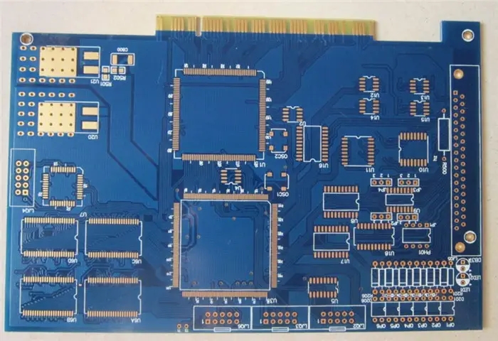
First, most PCB designers are profICient in the working principle of electronIC components, know their interaction, and better understand the various data transmission standards that constitute the input and output of the circuit board. An excellent electronic product needs not only excellent schematic diagrams, but also people who need PCB layout and wiring. The latter plays a crucial role in the final success of the circuit board. However, the more schematIC designers know about excellent layout technology, the more opportunities they have to avoid major problems.
Second, the handling of noise problems. With the improvement of PCB design speed, concurrent switching noise, concurrent switching output, ringing, crosstalk ground bounce and power supply noise also appear. To solve these problems, we need to suit the remedy to the case:
A. Ringing and crosstalk. For the key signal lines, we must pay attention to the crosstalk problem. The common way is to use differential signals and use differential pairs for routing. This can fundamentally eliminate the inductive effect and help reduce the "bounce" noise generated by the induced current in the return path.
B. Pay attention to impedance matching. I have done antenna matching circuit, and impedance matching plays a crucial role. Now 100 Ω characteristic impedance has become the industry standard value of differential connecting line. The 100 Ω difference line can be made of two 50 Ω single ended lines of equal length. Because the two lines are close to each other, the field coupling between lines will reduce the differential mode impedance of the line. In order to maintain an impedance of 100 Ω, the width of the wiring must be reduced a little. As a result, the common mode impedance of each line in the 100 Ω differential line pair will be a little higher than 50 Europes. If you really don't want to make such a fuss, you should negotiate with the manufacturer about what kind of impedance is required for wiring when making PCB.
C. Use of decoupling and bypass capacitors. In general, decoupling capacitors help reduce the inductance between the power supply of the PCB and the ground plane, and control the signals on the PCB and the impedance of the IC. The bypass capacitor provides a clean power supply (provides a charge bank). Generally, we should arrange decoupling capacitors anywhere convenient for PCB wiring. For the use of capacitors, it should be noted that the wiring of decoupling capacitors should be as short as possible.
Third, layout. We all know that the shortest and most direct path of the most critical connection design in PCB design can achieve the best effect with the SIMplest method. Why not?
Fourth, clock signal processing. I believe that PCB designers are experiencing or preparing for clock signal interference. Because the clock line is too long or passes through the signal line, jitter and offset will be amplified for the downstream, especially when the clock speed increases. First of all, PCB design should avoid using multiple layers to transmit the clock, and do not have vias on the clock line, because vias will increase the impedance change of the routing and signal reflection. Secondly, if the clock must be deployed in the inner layer, the upper and lower layers should use the ground plane to reduce the delay. Thirdly, if clock noise is unfortunately introduced on the power plane, which will increase PLL jitter, a "power island" can be created when modifying the PCB design. This technology can use thicker etching in the metal plane to achieve the isolation of PLL analog power supply and digital power supply.
Fifth, refer to the design scheme. Now any MCU will give its corresponding reference design. Although these circuit boards are usually designed for multiple purposes, they may not match your design requirements exactly. However, they can still be used as a starting point for creating solutions. We can see the routing and positioning of key parts, which is also a great improvement for the success rate of design. PCB manufacturers, PCB designers and PCBA manufacturers will introduce PCB design from shallow to deep.


抖音二維碼

Q Q二維碼

微信二維碼
點擊
然后
聯系
然后
聯系
電話熱線
13410863085Q Q

微信

- 郵箱