鑫景福致力于滿足“快速服務(wù),零缺陷,輔助研發(fā)”PCBA訂購單需求。


PCBA方案設(shè)計
Understand the design principles of PCBA board
The basIC process can be divided into three steps: PCB schematic design, net list generation, and PCB design Whether it is on the PCB assembly board or PCB trace, etc, There are specific requirements
For example, input and output wiring should be avoided as much as possible to avoid interference. The parallel wiring of two signal lines must be separated by ground wires, and the wiring of two adjacent layers should be as perpendicular to each other as possible. Parasitic coupling may occur in parallel. The power line and ground wire shall be divided into two layers as far as possible to be perpendicular to each other. As far as the line width is concerned, the wider ground wire can be used as the circuit of the digital Circuit PCB to form a grounding network (analog circuits cannot be used in this kind of pipe), and large areas of copper can be used.
The following article explains the principles and some details that should be paid attention to in the PCB design of the microcontroller control board.
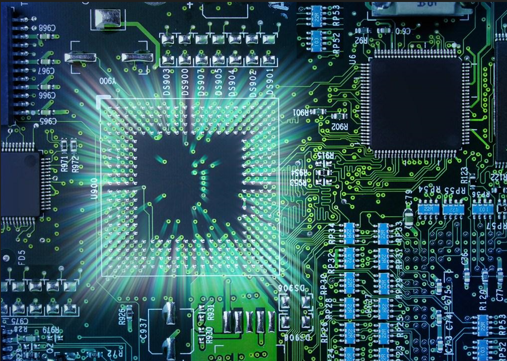
Circuit board

1. PCB assembly layout
In the component layout, the relevant components should be as close as possible. For example, clock generators, crystal oscillators and CPU clock inputs are prone to generate noise, so they should be placed closer together.
For those devices that are easy to generate noise, PCB current circuit, high current circuit switch circuit, etc, keep them away from the logic control circuit and storage circuit (ROM, RAM) of the microcontroller as much as possible. If possible, these circuits can be made into circuits Board, which is conducive to anti-interference and improves the reliability of circuit operation
2. Decoupling capacitor
Try installing decoupling capacitors next to key components such as ROM, RAM, and other chips. In fact, PCB traces, pin connections and wiring may contain large inductive effects. A large inductance may cause serious switching noise SPIkes on the Vcc path.
The only way to prevent switching noise spike on Vcc track is to place a 0.1uF electronic decoupling capacitor between Vcc and power grounding. If surface mount components are used on the circuit board, chip capacitors can be directly used on the components and fixed on the Vcc pin.
Ceramic capacitors are preferred because they have low electrostatic loss (ESL) and high frequency impedance, and the temperature and time of dielectric stability of such capacitors are also very good. Try not to use tantalum capacitors because they have higher impedance at high frequencies.
Please pay attention to the following points when placing decoupling capacitors:
3. PCB ground wire design
In the PCB single chip microcomputer control system, there are many types of ground wires, such as system ground wire, mask ground wire, logic ground wire, analog ground wire, etc. The reasonable layout of the ground wire will determine the anti-interference capability of the circuit board. When designing the ground wire and grounding point of PCB, the following issues should be considered:
4. Other
In addition to the layout of the power cord, the width of the trace should be as thick as possible according to the size of the current. In PCB layout design, the wiring direction of power line and ground line shall be consistent with that of data line. Finally, use the ground wire to cover the place where there is no trace at the bottom of the circuit board. These methods are helpful to improve the anti-interference ability of the circuit.
The width of the data line should be as wide as possible to reduce impedance. The width of the data line shall not be less than 0.3mm (12mil) at least, and it is better to use 0.46-0.5mm (18mil-20mil).
Because the through-hole on the circuit board will produce a capacitance effect of 10pF, which will cause too much interference to the high-frequency PCB circuit, the number of through-hole should be reduced as much as possible in PCB layout design In addition, too many vias will also reduce the mechanical strength of the circuit board


抖音二維碼

Q Q二維碼

微信二維碼
點擊
然后
聯(lián)系
然后
聯(lián)系
電話熱線
13410863085Q Q

微信

- 郵箱