鑫景福致力于滿足“快速服務,零缺陷,輔助研發”PCBA訂購單需求。


PCBA方案設計

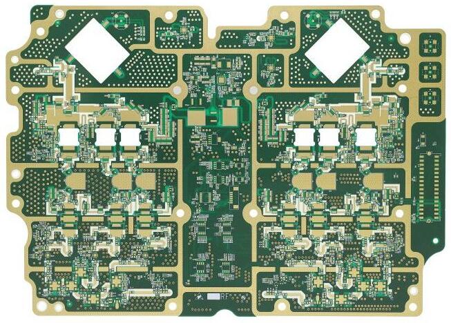
PCB board "integrated" products and schematIC diagram
Santa Cruz, California A startup initiated by Carnegie Mellon Univers, Inc. ity (CMU) researchers is preparing CircuitSpace, a PCB "synthesis" tool for printed circuit boards, claims to be the first tool PCB designer to place user assisted automation components on the tool By doing so, designAdvance Systems claims that it can reduce PCB design time by 50%
DesignAdvance (Pittsburgh, Pennsylvania) announced that it has formed an alpha test program with four partners and will launch Circuit Space at the PCB design meeting on March 7, 2005. Partners include Computerix Inc., EMA Design Automation, Laurel Networks, and Marconi Corp.
Circuit space allows designers to specify constraints, design rule checking (DRC), and power rule checking (ERC). It provides automatic and interactive constraint driven component placement, automatic bypass capacitor assignment, channel or port duplication, automatic clustering of key components and supporting circuits, and reuse of module library design.
The optimization algorithm can consider multiple constraints, including signal propagation delay, fixed component relationship, component direction, component symmetry, component height, thermal limit, manufacturability and power requirements.
DesignAdvance created Circuit Space and developed two patented platform technologies in CMU, including five patents. The company has received 2.4 million dollars of research funds from the National Science Foundation of the United States, United Technologies, General Motors, Ford, Daimler Chrysler and other commercial companies.
Randy Eager, CEO and co-founder of DesignAdvance, obtained a license from an official of CMU Technology Transfer Office. He worked for BASF and TriTech Group, an electronic packaging startup, and served as a management consultant for five years.
The inventors of DesignAdvance Technology include Jay McCormack, the co-founder and chief scientist, and Chandan Aladahalli, who have recently obtained a doctor's degree from CMU. Co founder and chief technology expert Jonathan Kagan is a professor of mechanical engineering at the University of Chicago.
How to reverse the schematic diagram of a PCB
Circuit board

In PCB reverse science and technology research, reverse push schematic refers to reverse push PCB file diagram or directly draw PCB circuit diagram according to actual products, aiming to explain the principle and working conditions of PCB. In addition, the circuit diagram is also used to analyze the functional characteristics of the product itself. In the forward design, general product development must first carry out schematIC design, and then carry out PCB design according to the schematic.
Whether it is used to analyze the circuit board principle and product operation characteristics in reverse research or reused in PCB design forward design, PCB schematics have a special role Therefore, how to reverse the PCB schematic diagram based on the file diagram or the actual object diagram, and what details should be paid attention to in the reverse calculation process?
1. Reasonably divide functional areas
When reverse designing the schematic diagram of a good PCB, reasonably dividing the functional area can help engineers reduce some unnecessary trouble and improve the drawing efficiency. Generally speaking, components with the same function on the PCB board are arranged in a centralized manner. When reversing the schematic diagram, it is convenient and accurate to divide the area according to the function.
However, the division of this functional area is not arbitrary. It requires engineers to have a certain understanding of electronic circuit related knowLEDge. First, find the core components in a functional unit, and then find other components of the same functional unit according to the wiring connection, thus forming a functional partition. The formation of functional partitions is the basis of schematic drawing. In addition, in this process, don't forget to skillfully use the serial numbers of components on the circuit board, which can help you divide functions faster.
2. Find the correct reference part
This reference part can also be said to be the city used at the beginning of the PCB network schematic diagram of the main components After determining the reference parts, drawing the reference parts according to the pins of these reference parts can ensure the accuracy of the schematic diagram to a greater extent Gender
It is not a very complicated thing for engineers to determine the reference parts. Under normal conditions, components that play a major role in the circuit can be selected as reference components. They are usually large in size and have many pins, making it easy to draw. For example, integrated circuits, transformers, transistors, etc. can be used as appropriate reference elements.


抖音二維碼

Q Q二維碼

微信二維碼
點擊
然后
聯系
然后
聯系
電話熱線
13410863085Q Q

微信

- 郵箱