鑫景福致力于滿足“快速服務,零缺陷,輔助研發”PCBA訂購單需求。


PCBA方案設計

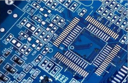
Many powerful out of the box development boards are also becoming more and more accessible, but many use cases still require the use of custom PCBs for electronIC product applications. In one-time development, even an ordinary pcb can play a very important role. PCB is the physical platform for design and the most flexible part for electronic system design of original components. This article will introduce several golden rules for PCB design. Since the commercial PCB design was born 25 years ago, most of these rules have not changed and are widely applicable to various PCB design projects. These rules have a great guiding role for young electronIC design engineers and more mature circuit board manufacturers.
The following content of this paper introduces the ten most effective design principles that electronic design engineers should remember and practice when using design software for PCB layout design and commercial manufacturing. Engineers do not need to implement these rules in chronological order or relative importance, but they can greatly change the product design by following them all.
Rule 1:
Select the correct grid - set and always use the grid spacing that matches the most components. Although the multi grid seems to be of great utility, if engineers can think more at the beginning of PCB layout design, they can avoid difficulties in interval setting and can maximize the application of circuit boards. Since many devices use a variety of package sizes, engineers should use products that are most conducive to their own design. In addition, polygons are very important for copper coating on circuit boards. Multi grid circuit boards generally have polygon filling deviation when copper coating on polygons. Although it is not as standard as that based on a single grid, it can provide more than the required service life of circuit boards.
Rule 2:
Keep the path shortest and most direct. This sounds SIMple and common, but it should be kept in mind at every stage, even if it means changing the circuit board layout to optimize the wiring length. This is especially applicable to analog and high-speed digital circuits where the system performance is always partially limited by impedance and parasitic effects.
Rule 3:
Use the power layer to manage the distribution of power lines and ground wires as much as possible. Copper coating on the power supply layer is a fast and simple choice for most PCB design software. By connecting a large number of conductors together, it is ensured that the current with the highest efficiency and minimum impedance or voltage drop is provided, while providing an adequate return path to ground. If possible, multiple power supply lines can also be run in the same area of the circuit board to confirm whether the ground plane covers most of the layers of a PCB layer, which is conducive to the interaction between running lines on adjacent layers.
Rule 4:
Group the relevant components together with the required test points. For example, the discrete components required by the OpAmp operational amplifier are placed close to the device so that the bypass capacitor and resistance can cooperate with them on the same ground, which helps optimize the wiring length mentioned in Rule 2, and also makes testing and fault detection easier.
Rule 5:
Copy the required circuit board on another larger circuit board for multiple tiMES for PCB assembly. Selecting the size most suitable for the equipment used by the manufacturer is conducive to reducing prototype design and manufacturing costs. First, lay out the circuit board on the panel, contact the Circuit board manufacturer to obtain their preferred size specifications for each panel, then modify your design specifications, and try to repeat your design multiple times within these panel sizes.
Rule 6:
Integrate component values. As a PCB designer, you will select some discrete components with high or low component values but the same performance. By consolidating within a SMAller range of standard values, the bill of materials can be simplified and costs may be reduced. If you have a series of PCB products based on the preferred device value, it will also help you to make correct inventory management decisions in the longer term.
Rule 7:
Perform PCB design rule checking (DRC) as much as possible. Although it only takes a short time to run DRC functions on PCB software, in more complex design environments, as long as you always perform checks during the design process, you can save a lot of time, which is a good habit worth keeping. Every cabling decision is critical, and you can always be rEMInded of the most important cabling by executing DRC.
Rule 8:
Flexible use of screen printing. Screen printing can be used to MARK various useful information for future use by circuit board manufacturers, service or test engineers, installers or equipment commissioning personnel. Not only clearly mark the function and test point labels, but also indicate the direction of components and connectors as much as possible, even if these notes are printed on the lower surface of components used in the circuit board (after the circuit board is assembLED). The full application of screen printing technology on the upper and lower surfaces of circuit boards can reduce repetitive work and streamline the production process.
Rule 9:
Decoupling capacitor is required. Do not attempt to optimize your design by avoiding decoupling power lines and following the limits in the PCB component data sheet. Capacitors are cheap and durable. You can spend as much time as possible to assemble them, while following Rule 6 and using the standard value range to keep the inventory neat.
Rule 10:
Generate PCB manufacturing parameters and verify them before submitting to production. Although most circuit board manufacturers are happy to download and verify for you directly, you'd better output Gerber files first and check whether they are as expected with a free reader to avoid misunderstanding. Through personal verification, you will even find some careless mistakes, and thus avoid losses caused by completing production according to the wrong parameters.
As circuit design sharing becomes more and more extensive, and internal teams increasingly rely on reference design, basic rules like the above will still be a feature of PCB design, which we believe is very important for PCB design. By clarifying these basic rules, developers can be very flexible to enhance the value of their PCB products and get the maximum benefit from the circuit boards they manufacture.


抖音二維碼

Q Q二維碼

微信二維碼
點擊
然后
聯系
然后
聯系
電話熱線
13410863085Q Q

微信

- 郵箱