鑫景福致力于滿足“快速服務,零缺陷,輔助研發”PCBA訂購單需求。


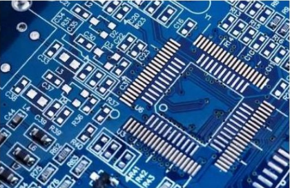
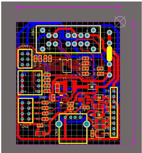
PCBA方案設計
The sensitivity of PCB devices is getting higher and higher, whICh requires that the anti-interference ability of devices is also getting stronger and stronger, so PCB design becoMES more difficult. How to improve the anti-interference ability of PCB has become one of the key issues that many engineers pay attention to. This paper will introduce some tips to reduce noise and electromagnetic interference in PCB design.
The following are 24 tips for reducing noise and electromagnetic interference in PCB design summarized through years of design:
(1) If you can use low-speed chips, you don't need high-speed ones. High speed chips are used in key places.
(2) A series of resistors can be used to reduce the jumping rate of the upper and lower edges of the control circuit.
(3) Try to provide some form of damping for relays, etc.
(4) Use the clock with the lowest frequency meeting the system requirements.
(5) The clock generator shall be as close as possible to the device using the clock. The shell of quartz crystal oscillator shall be grounded.
(6) Circle the clock area with a ground wire and keep the clock wire as short as possible.
(7) The I/O drive circuit shall be close to the edge of the PCB as far as possible, so that it can leave the PCB as soon as possible. The signal entering the PCB shall be filtered, and the signal coming from the high noise area shall also be filtered. At the same time, the serial terminal resistance shall be used to reduce the signal reflection.
(8) The useless end of MCD shall be connected high, or grounded, or defined as an output end. The power supply and ground terminals on the integrated circuit shall be connected, and shall not be suspended.
(9) The unused gate circuit input terminal shall not be suspended, the unused op amp positive input terminal shall be grounded, and the negative input terminal shall be connected to the output terminal.
(10) As far as possible, the printed PCB board uses 45 fold lines instead of 90 fold lines to reduce the external transmission and coupling of high-frequency signals.
(11) The printed circuit board shall be partitioned according to the frequency and current switching characteristics, and the noise components shall be further away from the non noise components.
(12) Single point power supply and single point grounding, power line and ground wire shall be as thick as possible for PCB single panel and double panel. If the economy is affordable, multi-layer boards shall be used to reduce the inductance of power supply and ground.
(13) The clock, bus and chip selection signals shall be far away from I/O lines and connectors.
(14) Analog voltage input line and reference voltage terminal shall be far away from digital circuit signal line, especially clock.
(15) For A/D devices, the digital part and the analog part should be unified rather than crossed.
(16) The clock line perpendicular to the I/O line has less interference than the parallel I/O line, and the clock element pin is far away from the I/O cable.
(17) PCB component pin shall be as short as possible, and decoupling capacitor pin shall be as short as possible.
(18) The key lines should be as thick as possible, and protective areas should be added on both sides. High speed lines should be short and straight.
(19) The lines sensitive to noise shall not be parallel to the high current and high-speed switching lines.
(20) Do not run wires under quartz crystal or noise sensitive devices.
(21) Do not form a current loop around the weak signal PCB circuit and low-frequency circuit.
(22) The signal shall not form a loop. If it is unavoidable, the loop area shall be as SMAll as possible.
(23) Each integrated circuit has a decoupling capacitor. A small high-frequency bypass capacitor shall be added beside each electrolytic capacitor.
(24) Use high-capacity tantalum capacitors or Juku capacitors instead of electrolytic capacitors as circuit charging and discharging energy storage capacitors. When using tubular capacitors, the enclosure should be grounded.
Do you know the eternal PCB design rules
11-19,2022


抖音二維碼

Q Q二維碼

微信二維碼
點擊
然后
聯系
然后
聯系
電話熱線
13410863085Q Q

微信

- 郵箱