鑫景福致力于滿足“快速服務,零缺陷,輔助研發”PCBA訂購單需求。


PCBA方案設計

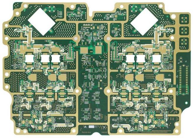
Files required by PCB to be sent to SMT factory
The following mainly introduces that PCB boards are sent to SMT chip processing plants
1、 Files required
1. BOM parts list
2. No welding list
3. SMT coordinate file
4. DevICe schematic diagram
5. Manual welding parts list
6. Make die file PCB
2. Description of the steps and methods of making each file
1. BOM parts list
2. No welding list
3. SMT coordinate file
4. Product silk screen image (DXP is recommended)
(1) Schematic Diagram of Top Surface Parameters
(2) Top Digital Diagram
(3) Schematic Diagram of Bottom Parameters
(4) , Schematic Diagram of Bottom Parameters
5. Manual welding parts list
6. PCB steel wire MESh file
3. DetaiLED description of production steps and methods for each file
Circuit board

1. BOM parts list
Production method: export in schematic diagram and organize
Export method: protel and DXP have the same method. It is recommended to export in DXP
Select [Reports/Bill of Material] on the interface, and then directly select Next until Finish
2. No welding list
Organize according to the first step component list
3. Methods and steps for exporting SMT coordinate files:
(1) Select [File/Open – Open the. PCB file;
(2) , click TopLayer, and select [Edit/Select/All on Layer] on the layer;
(3) , click BottomLayer, and select [Edit/Select/All on Layer] on the layer;
(4) When finished, press Shift+Delete to delete the redundant lines at the top and bottom;
(5) Select [design/Options -), open the Layers button, select [Toplayer]/[BottomLayer] under Singal Layers, select [Top Overlay]/[BottomLayer] under Silkscreen, and then select Other under [Keepout];
Note: You can also turn off Top and Bottom separately to make them clearer.
(6) After the above steps are completed, the position of the pad screen can be clearly displayed;
(7) Select [Edit/Origin/Setting] to set the origin position (* After setting the PCB origin position, remember that the PCB origin position on the machine should also be set here);
(8) Select [File/CA. M Manager] In the export wizard, select a pick location, select text, continue to click Next, select Metric as the organization, and complete the generation of the pick location file. Select and press F9 to generate the CAM file;
(9). Find the pickup location.. In CAM.. In the directory of the Data Manager window on the left, right-click and export to the desired target path;
(10) Then use Excel to open the picking location file and organize it into the file required by SMT, where Mid X and Mid Y are the X and Y coordinates required by SMT.
Note: The top floor and bottom floor shall be separated during sorting
4. Pdf file of screen printing drawing of product part position (DXP is recommended)
(1) Schematic Diagram of Top Surface Parameters
The schematic diagram of the top surface parameters is the resistance and capacitance of the topology layer, the resistance value and capacitance value of the IC, the name of the IC, etc. (10K, 1UF, MAX354, etc.)
Note: All parameters should be centered (within the wire mesh of the mat)
Steps and methods:
A. Open PCB file in DXP
B. Select to display only TopOverlay and KeepOutLayer
C. Hide the equipment number and only display the device parameters. Put the parameters of each equipment in the wire mesh of the mat and in the middle. Pay attention to the consistency of the order and direction
D. Select [File/SMArt PDF – PDF] to export as a PDF file
Note: Figures 2, 3 and 4 indicate that only TopOverlay and KeepOutLayer layers are selected for output
Left click to select layer, right click to select delete layer and add layer
Delete is to delete a layer; Inserting a layer is to add a layer
(2) Top Digital Diagram
The schematic diagram of the number of top surfaces is the resistance, capacitance and IC number of topological layers (R1, C1, U1, etc.)
Note: All digits should be centered (within the screen of the mat)
Steps and methods:
A. Open PCB file in DXP
B. Select to display only TopOverlay and KeepOutLayer
C. Hide the equipment parameters and only display the device number. Put the number of each equipment in the wire mesh of the mat and in the middle. Pay attention to the consistency of the order and direction
D. Select [File/Smart PDF – PDF] to export as a PDF file
The details are the same as the first step above
(3) Schematic Diagram of Bottom Parameters
The schematic diagram of bottom parameters shows the resistance, capacitance, IC resistance, capacitance, IC name, etc. of the bottom covering layer (10K, 1UF, MAX354, etc.)
Note: All parameters should be centered (within the wire mesh of the mat)
Steps and methods:
A. Open PCB file in DXP
B. Select to display BottomOverlay and KeepOutLayer only
C. Hide the equipment number and only display the device parameters. Put the parameters of each equipment in the wire mesh of the mat and in the middle. Pay attention to the consistency of the order and direction
D. Select [File/Smart PDF – PDF] to export to PDF file
The detailed steps are basically the same as the first step above
(4) , Schematic Diagram of Bottom Parameters
The figure on the bottom is the number of resistors, capacitors and ICs of the bottom covering layer (R1, C1, U1, etc.)
Note: All digits should be centered (within the screen of the mat)
Steps and methods:
A. Open PCB file in DXP
B. Select to display BottomOverlay and KeepOutLayer only
C. Hide the equipment parameters and only display the device number. Put the number of each equipment in the wire mesh of the mat and in the middle. Pay attention to the consistency of the order and direction
D. Select [File/Smart PDF – PDF] to export as a PDF file
The details are the same as in step 3 above
5. Manual welding parts list
Organize according to BOM
6. PCB steel mesh file
This file is provided by the hardware department


抖音二維碼

Q Q二維碼

微信二維碼
點擊
然后
聯系
然后
聯系
電話熱線
13410863085Q Q

微信

- 郵箱