鑫景福致力于滿足“快速服務(wù),零缺陷,輔助研發(fā)”P(pán)CBA訂購(gòu)單需求。


PCBA方案設(shè)計(jì)
Relevant details of circuit board design company
designing a good PCBA board is our fundamental source According to the overall structure, the size and structure shape of PCBA are determined by using the electrICal principle and mechanical structure design Draw the outline process diagram of SMT printed board, MARK the length, width, PCB thickness, position and size of structural components, assembly holes, and reserve the edge size, so that the circuit designer can carry out wiring design within the effective range The selection of assembly type depends on the type of components in the circuit, the size of the circuit board and the equipment conditions of the production line Selection principle of PCB assembly form: follow the principle of optimizing process, reduce cost and improve product quality First, determine the overall goal, performance index, cost and overall size of the electronic product Product performance positioning, quality and cost
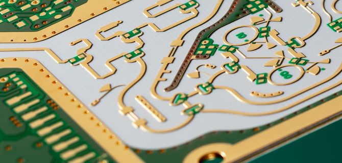
Circuit board

-Under normal circumstances, any product design needs to balance and compromise efficiency, manufacturability and cost Therefore, the use and grade of products must be put in the first place in design PCB design is complex, and various unexpected factors often affect the implementation of the overall solution How can we overcome these different problems? How can we draw a clean, efficient and reliable PCBA board? We are a professional pcb design company PCBA board design It is necessary to consider the direction of various signals and the transmission of energy But in fact, it is clear that the summary can start from two aspects: frankly, it is: "how to place" and "how to connect" 1. Follow the layout principle of "large before SMAll", Difficult before easy "That is, priority should be given to important unit circuits and core components. It is like eating a buffet: the appetite of the buffet is limited to selecting favorite foods, and the design space of the PCB is limited to picking up important pendants. 2. The layout should refer to the schematic diagram and arrange the main components according to the main signal flow direction of the PCB design. The layout should try to meet the following requirements: the total connection should be as short as possible, the key signal lines should be as short as possible, and the decoupling capacitor should be The layout shall be as close as possible to the power supply pin of the integrated circuit, and the loop formed between the power supply and the ground shall be as short as possible; Prevent road accidents 3. The Layout of components should be easy for debugging and maintenance, that is, there should be no large components around small components, and there must be enough space around the components to be debugged, while overcrowding often becoMES very embarrassing The heating elements should be approximately evenly distributed In order to facilitate the heat dissipation of the single board and the whole machine, temperature sensing elements other than temperature detection elements should be far away from high-temperature elements 5. For circuit parts with the same structure, try to adopt the "symmetrical" standard layout; Optimize the layout according to the uniform distribution standard, balance the center of gravity, and make the layout beautiful 6. Plug in components of the same type shall be placed in one direction along the X or Y direction The same type of polar discrete elements must also be consistent in the X or Y direction for ease of production and inspection 7. High voltage and high current signals are separated from low current and low voltage weak signals; Separation of analog signal and digital signal; Separation of high frequency signal and low frequency signal; High frequency components are spaced sufficiently When handling components, equipment with the same power supply shall be put together as much as possible to separate the power supply in the future The main consideration of "how to place" layout "How to connect" is relatively more complex. The priority of key signal lines: analogy to the priority routing of key signals, such as small signals, high-speed signals, clock signals and synchronization signals; Density priority principle: from design to PCBA board Wire from the densest area of the circuit board
Wiring is an important step in PCB product design. The cabling design process is the most rigorous, with the best skills and the largest workload. It can be said that the previous preparations have been completed. The PCBA layout is divided into three types: single-sided wiring, double-sided wiring and multi-layer wiring. PCBA layout can be completed using automatic and manual routing provided by the system. Although the system provides designers with convenient operation and automatic wiring with high wiring rate, there are still unreasonable points in the actual design. At this point, the designer needs to manually adjust the wiring on the PCBA to obtain the best results. The quality of PCBA Design has a great influence on its anti-interference ability. It must conform to the basic principles of design and meet the requirements of anti-interference design to achieve the best efficiency of the circuit.
The wire of printed circuit board shall be as short as possible; The address line or data line of the unified component shall be as long as possible; When the circuit is high-frequency circuit or the wiring is dense, the corner of the printed wire shall be round. Otherwise, it will affect the electrical characteristics of the circuit. When wiring on both sides, the conductors on both sides shall be perpendicular, inclined or bent to each other to avoid parallelism and reduce parasitic coupling. PCB shall use 45 ° fold line instead of 90 ° fold line to reduce the coupling between external transmission and high-frequency signal. As the input and output of the circuit, the printed circuit should avoid backflow as much as possible, and it is better to add a grounding wire between these lines. When the wiring density on the board surface is high, the mesh copper foil shall be filLED with a grid size of 02mm (8mil).
SMD pads cannot be placed through holes to avoid solder paste loss caused by component solder joints. It is not allowed to pass through important signal lines between sockets. Avoid installing resistors, inductors (inserts), electrolytic capacitors and other components horizontally below the hole to avoid short circuit between the hole and the component housing after peak welding. For manual wiring, first place the power cord on the ground wire, and the power cord should be on the same horizontal plane. The signal cable shall not have loopback wiring. If you need a loop, make the loop as small as possible. When wiring passes between two pads but is not connected to them, they should be kept at a large and equal spacing. The distance between wiring and conductors shall also be uniform, equal and maximum. The connection between the conductor and the gasket shall be too smooth to avoid small sharp corners. When the center distance between pads is less than the outer diameter of one pad, the width of connecting lines between pads can be the same as the diameter of pads; When the center distance between pads is greater than the outer diameter of pads, the width of welding wire shall be reduced; When there are more than 3 pads on the wire, the distance between them should be greater than the width of two diameters. The common grounding of printed circuit shall be placed on the edge of PCB as far as possible.
The copper foil should be kept on the PCB as much as possible. In retrOSPect, the shielding effect is better than the long grounding wire It will also improve transmission line characteristics and mask effect, and realize the function of reducing distributed capacitance The common grounding of the printed conductor is preferably formed into a ring or network, because when there are many integrated circuits on the same PCB, due to the limitation of the pattern, there will be a ground potential difference, which will reduce the noise tolerance When a loop is formed, the ground potential difference decreases To suppress noise, ground and power modes should be parallel to the data flow as much as possible multilayer PCBA can use multiple layers as mask layers PCB power layer and PCB ground plane can be regarded as mask layer

Overview of PCBA Board Industry Development
11-20,2022


抖音二維碼

Q Q二維碼

微信二維碼
點(diǎn)擊
然后
聯(lián)系
然后
聯(lián)系
電話熱線
13410863085Q Q

微信

- 郵箱