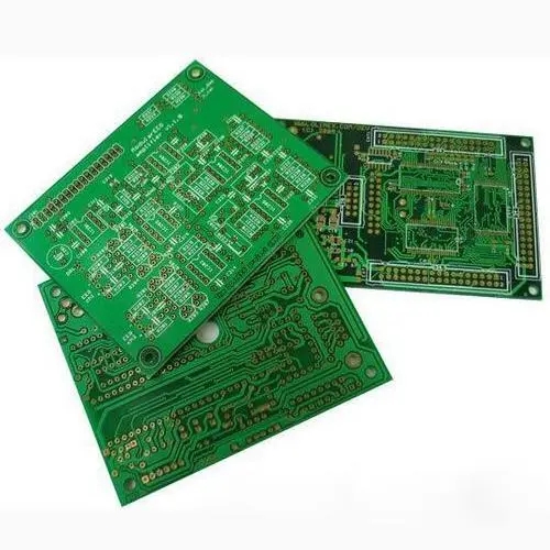
鑫景福致力于滿足“快速服務(wù),零缺陷,輔助研發(fā)”PCBA訂購單需求。


PCBA方案設(shè)計(jì)
Five problems in mICrowave/RF PCB high frequency board design
circuit board manufacturing, circuit board design and PCBA processing manufacturers explain five problem solutions for microwave/RF PCB high-frequency Board Design
With the ability of microwave and RF PCB high frequency board design to capture higher frequencies, its importance is self-evident. Microwave and RF circuits have become a part of various products, among which communication equipment is the most attractive. For microwave and RF High Frequency Circuit Boards, a large number of manufacturing is completed for different devices. However, the higher frequency also brings many high frequency circuit board design challenges. Here are some convenient solutions to alleviate some of these problems:
1. Effective techniques for designing microwave RF PCB
Please pay attention to using these microwave circuit board/RF PCB design techniques to ensure that the possibility of any errors can be minimized during the assembly process:
Isolation - If you are dealing with high-frequency PCBs with analog, digital, and RF components, one thing you need to pay attention to at the design stage is to separate these components. U Ground plane - In the case of multilayer PCB (RF PCB/microwave circuit board/high-frequency circuit board), a rule of thumb is that there is a ground plane below any layer with RF or microwave signal lines.
Solution to noise - Since high-frequency signals are extremely sensitive to noise, there are several solutions:
Shot Noise - This noise caused by current fluctuations can be minimized by using metal resistors.
Phase Noise - Affects RF signals in the form of fluctuations or phase jitters. Clean signals are the best way to reduce this noise.
Flicker noise - caused by DC current, this noise appears as phase noise. The solution is to process the signal through special filters.
Thermal noise - This noise is the result of thermal agitation. Therefore, the temperature must be adjusted through the cooling system and heat dissipation function to minimize the impact of temperature on the circuit.
Avalanche noise - This noise is due to the fact that the junction diode operates near the avalanche breakdown point. The best solution for this is to use a capacitor based filter.
2. Return loss
Due to signal reflection, the method to minimize return loss is to ensure that the ground plane from the driver to the receiver should be continuous. Without this, the return signal will pass through other power planes and cause signal noise.
3. RF PCB/microwave circuit board/high-frequency circuit board impedance matching
Due to the low tolerance of high-frequency signals to impedance matching, the following aspects should be noted:
Skin effect loss skin effect refers to the flow of electrons along the external surface at higher frequencies. On the trace, there is a SMAll region for funnel electrons. However, some electrons are also trapped here. The signal energy is converted into heat. In order to minimize this loss, proper impedance matching is essential. In addition, gold plated PCB can also be used as an antidote.
Line length - signal loss is affected by line length. The longer the line, the more signal loss. It is better to ensure that the line is 1/20 of the wavelength. Either way, it should be longer than 1/16 of the wavelength, which is the critical signal length.
4. Intermodulation distortion
In short, crosstalk is the transfer of energy between conductors leading to coupLED signals. Generally, the incidence of crosstalk increases with the increase of PCB density and performance. Other areas that play a role include:
Proximity of conductor
The distance of their parallel operation
Edge rate of active line
Some ways to reduce crosstalk include:
Make sure that the distance from the center to the center is four tiMES the width of the route.
Minimize parallel lines
Minimize dielectric spacing
Insert ground plane between routes
End the line at its characteristic impedance
5. Microwave and RF laminate performance
The characteristics of the laminate will affect the function of RF or microwave PCB/RF circuit board. For example, FR4 fiberglass board has a high dissipation factor, resulting in higher insertion loss as the signal frequency increases. In addition, the dielectric constant of FR4 is higher than that of the high-frequency laminate, which has an impact on the impedance. The characteristics of the laminate affect the dielectric loss. It is recommended to use a substrate with a low loss factor to avoid this loss.
This is a method to solve the common problems of microwave and RF PCB/microwave circuit board/high-frequency circuit board design and improve its efficiency!


抖音二維碼

Q Q二維碼

微信二維碼
點(diǎn)擊
然后
聯(lián)系
然后
聯(lián)系
電話熱線
13410863085Q Q

微信

- 郵箱