鑫景福致力于滿足“快速服務,零缺陷,輔助研發”PCBA訂購單需求。


PCBA方案設計
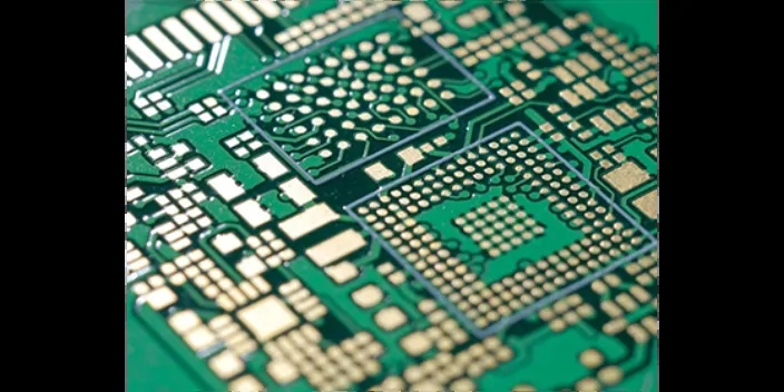
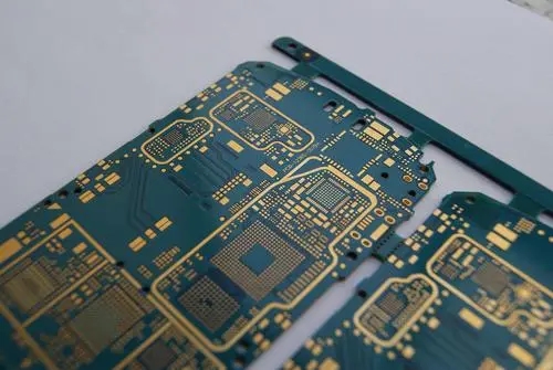
Calculation Impedance of High Frequency PCB and Electroplating Problems
PCB manufacturers, PCB designers and PCBA manufacturers will explain the calculated impedance and electroplating of high-frequency PCB
In the design of high frequency PCB, the impedance of high frequency PCB is an inevitable problem. What details should be paid attention to in the design and calculation of high frequency PCB?
1. The PCB line width of the high-frequency board would rather be wide than thin.
Because there is a limit of thinness in the PCB manufacturing process of high-frequency boards, there is no limit of width. In the later stage, it will be troublesome to thin the line width in order to adjust the impedance and meet the limit, whICh will lead to either increasing costs or relaxing impedance control.
2. There is an overall trend.
There may be multiple impedance control targets in the PCB design process of the high-frequency board, so the overall impedance control target should be larger or SMAller, and the asynchronous impedance control target should not be larger or smaller.
3. Consider copper residue rate and glue flow.
When one or both sides of the prepreg are etching lines, the glue will fill the etched gap during the pressing process, so that the glue thickness time between the two layers will be reduced. If the calculation of copper residue rate and glue flow is not accurate, and the dielectric coefficient of the new material is inconsistent with the nominal value, signal integrity problems may occur.
4. Specify glass cloth and glue content.
The dielectric coefficients of the prepreg or core plate with different glass cloth and different glue content are different. Even those of the same height may be 3.5 and 4, which can cause the change of the single line impedance of about 3ohm. In addition, the glass fiber effect is closely related to the window opening size of the glass cloth. If the design is 10Gbps or higher speed, and the laminated layer has no specified material, if the board factory uses a single piece of 1080PP material, there may be a signal integrity problem. Therefore, the R&D engineer must calculate what kind of PP is suitable for the design. If you need parameters, you can discuss with me.
Of course, the calculation of residual copper rate and glue flow is not accurate, the dielectric coefficient of new materials is sometiMES inconsistent with the nominal value, and some glass cloth plants do not prepare materials, which will cause the design lamination to be realized or the delivery date to be delayed. At the beginning of design, the best way is to let the board factory design the stack according to our requirements and their experience, so that the ideal and achievable stack can be obtained at most several times. The above is the method for designing and calculating impedance of high frequency PCB. I hope it can help you.
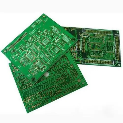
Analysis and elimination of problems in electroplating of high-frequency circuit boards
1、 Copper plating of high-frequency circuit board has local leakage or step plating
1) Cause The content of organic matters in the plating solution is too much. Treatment measures: treat the copper plating solution with activated carbon.
2) The reason is that the dry film development is not clean. Treatment measures: recheck the development conditions of the dry film.
3) The High Frequency Circuit Board has been polluted by fingerprints and oil stains. Treatment measures: increase the temperature of degreasing bath solution before electroplating.
4) Cause The dry film surface exudes residue of developer. Treatment measures: After development, it must be placed for 30 minutes before electroplating to balance the reaction.
2、 Causes and treatment of poor adhesion between copper plating layers of high-frequency circuit board
1) Cause Insufficient water washing after dry film development. Treatment measures: check the dry film process and water washing conditions of development and improve them.
2) Cause: When the high-frequency circuit board enters the plating bath, the power supply is not turned on. Treatment measures: Recheck the automatic procedure of rectifier.
3) Cause: the wetting agent in the oil cylinder is brought out or the water washing is insufficient, resulting in the passivation of the bottom copper. Treatment measures: check the water washing procedure, increase the water washing flow and increase the washing water temperature.
4) Cause: improper cleaning treatment before electroplating, and the oxidation or passivation film on the surface of the bottom copper was not removed. Treatment measures: increase the temperature of oil removal tank liquid to facilitate the removal of oil stains and fingerprints, check the activity of oil removal tank and micro etching tank liquid and improve them. PCB manufacturers, PCB designers and PCBA manufacturers will explain the calculation impedance and electroplating of high-frequency PCB.


抖音二維碼

Q Q二維碼

微信二維碼
點擊
然后
聯系
然后
聯系
電話熱線
13410863085Q Q

微信

- 郵箱