鑫景福致力于滿足“快速服務,零缺陷,輔助研發”PCBA訂購單需求。


PCBA方案設計
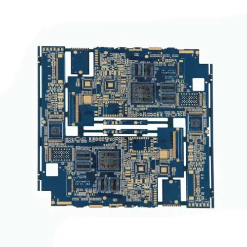
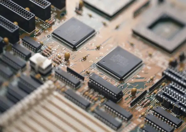
Introduction of Copper Cladding Method in PCB Design
PCB manufacturing, PCB design and PCBA processing manufacturers will explain the copper coating method in PCB design
Copper coating is an important part of PCB design. Whether it is a doMEStIC PCB design software or some foreign PowerPCBs, Protel has provided the intelligent copper coating function. So how to apply copper? I will share some of my ideas with you, hoping to bring benefits to peers.
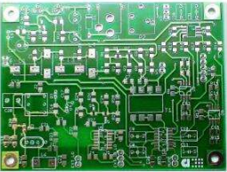
Copper coating is to use the idle space on the PCB as the reference plane and then fill it with solid copper. These copper areas are also calLED copper filling. The significance of copper coating is to reduce the ground wire impedance and improve the anti-interference capability; Reduce voltage drop and improve power efficiency; Connecting with the ground wire can also reduce the loop area. For the purpose of keeping PCB from deforming as much as possible during welding, most PCB manufacturers also require PCB designers to fill the open area of PCB with copper sheet or grid shaped ground wire. If copper coating is handled improperly, there will be no reward or loss. Is copper coating "more beneficial than harmful" or "more harmful than beneficial"?
As we all know, the distributed capacitance of the wiring on the printed circuit board will play a role in high frequency. When the length is greater than 1/20 of the corresponding wavelength of the noise frequency, the antenna effect will be generated, and the noise will be EMItted through the wiring. If there is a poorly grounded copper coating in the PCB, the copper coating will become a tool to spread the noise. Therefore, in high frequency circuits, do not think that the ground wire is grounded somewhere, This is the "ground wire", which must be less than λ/ 20, make holes on the wiring, and "well grounded" with the ground plane of the multilayer board. If the copper coating is properly treated, it not only increases the current, but also plays a dual role in shielding interference.

Generally, there are two basic methods of copper cladding, namely, large-area copper cladding and grid copper cladding. It is often asked whether large-area copper cladding or grid copper cladding is better. Why? Large area copper coating has the dual functions of increasing current and shielding. However, if large area copper coating is used for wave soldering, the board may be warped or even blistered. Therefore, for a large area of copper coating, several grooves are usually opened to alleviate the blistering of copper foil. The SIMple grid copper coating is mainly used for shielding, and the effect of increasing current is reduced. From the perspective of heat dissipation, the grid is beneficial (it reduces the heating surface of copper) and plays a certain role in electromagnetic shielding. However, it should be pointed out that the grid is composed of lines in staggered directions. We know that for circuits, The width of the wiring has its corresponding "electrical length" for the operating frequency of the circuit board (the actual size is divided by the digital frequency corresponding to the operating frequency, see the relevant books for details) When the working frequency is not very high, perhaps the role of grid lines is not very obvious. Once the electrical length matches the working frequency, it is very bad. You will find that the circuit does not work properly at all, and there are signals everywhere that interfere with the work of the system. Therefore, for colleagues who use grid, my suggestion is to choose according to the working conditions of the designed circuit board, instead of holding on to something. Therefore, high-frequency circuit requires high anti-interference multi-purpose grid, and low-frequency circuit has high current circuit and other commonly used complete copper coating.
With all that said, what problems should we pay attention to in order to achieve the desired effect of copper cladding:
1. For the single point connection of different ground, the method is to connect through a 0 ohm resistance or magnetic bead or inductance;
2. Copper clad near the crystal oscillator. The crystal oscillator in the circuit is a high-frequency emission source. The method is to copper clad around the crystal oscillator, and then ground the shell of the crystal oscillator separately.
3. If the problem of isolated islands (dead zones) is very big, it doesn't take much to define and add individual vias.
4. At the beginning of wiring, the ground wire should be treated equally. When wiring, the ground wire should be well laid. It is not possible to eliminate the connected ground pin by adding vias after copper coating. Such effect is very bad.
5. It is better not to have a sharp angle (less than or equal to 180 degrees) on the board, because from the electromagnetic point of view, this constitutes a transmitting antenna! For others that will always have an impact, it is just big or SMAll. I suggest using the edge line of the arc.
6. If there are many PCBs with ground, such as SGND, AGND, GND, etc., the most important "ground" shall be used as the reference for independent copper coating according to the different positions of the PCB board, and the digital and analog copper coating shall be separated. At the same time, before copper coating, the corresponding power lines shall be thickened: 5.0V, 3.3V, etc. In this way, multiple deformation structures with different shapes are formed.
7. The open area of the wiring in the middle layer of the Multilayer board shall not be covered with copper. Because it is difficult for you to make this copper clad "well grounded".
8. The metal inside the equipment, such as metal radiator and metal reinforcing strip, must be "well grounded".
9. The heat dissipation metal block of the three terminal voltage regulator must be well grounded. The grounding isolation belt near the crystal oscillator must be well grounded. If the grounding problem of copper coating on PCB is solved, it must be "more advantages than disadvantages". It can reduce the return area of signal lines and reduce the external electromagnetic interference of signals. PCB manufacturing, PCB design and PCBA processing manufacturers will explain the copper coating method in PCB design.


抖音二維碼

Q Q二維碼

微信二維碼
點擊
然后
聯系
然后
聯系
電話熱線
13410863085Q Q

微信

- 郵箱