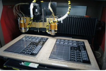
鑫景福致力于滿足“快速服務,零缺陷,輔助研發”PCBA訂購單需求。


PCBA方案設計
In the EMC design consideration of PCB, the first thing involved is the layer setting; The number of layers of a single board consists of the number of layers of power supply, ground and signal; In the EMC design of products, in addition to the selection of components and circuit design, good PCB design is also a very important factor.
The key to EMC design of PCB is to reduce the reflow area as much as possible, so that the reflow path flows in the direction we designed. The layer design is the basis of PCB. How to do a good job in PCB design to make PCB EMC better?

1. Design idea of PCB layer:
The core of the EMC planning and design idea for PCB stack is to reasonably plan the signal return path, minimize the return area of the signal from the mirror layer of the board as much as possible, and make the magnetIC flux cancellation or minimization.
1. Board image layer
The mirror layer is a complete copper-clad plane layer (power layer, ground plane) adjacent to the signal layer inside the PCB. It mainly has the following functions:
(1) Reduce the return noise: The mirror layer can provide a low impedance path for the return of the signal layer, especially when there is a large current flow in the power distribution system, the role of the mirror layer is more obvious.
(2) Reduce EMI: the existence of the mirror layer reduces the area of the closed loop formed by the signal and return flow, and reduces EMI;
(3) Reduce crosstalk: it is helpful to control the crosstalk between signal lines in high-speed digital circuits. Changing the height of signal lines from the mirror layer can control the crosstalk between signal lines. The SMAller the height, the smaller the crosstalk;
(4) Impedance control to prevent signal reflection.

2. Selection of mirror layer
(1) Power supply and ground plane can be used as reference plane, and have a certain shielding effect on internal wiring;
(2) Relatively speaking, the power plane has a high characteristic impedance, a large potential difference with the reference level, and a relatively large high-frequency interference on the power plane;
(3) From the perspective of shielding, the ground plane is generally grounded, and as the reference point of the reference level, its shielding effect is far better than the power plane;
(4) When selecting the reference plane, the ground plane shall be preferred, and the power plane shall be selected next.
3. Principle of magnetic flux cancellation:
According to Maxwell's equation, all electric and magnetic actions between discrete charged bodies or currents are transmitted through the middle area between them, no matter whether the middle area is vacuum or solid matter. In PCB, the magnetic flux always propagates in the transmission line. If the RF return path is parallel and close to its corresponding signal path, the magnetic flux on the return path and the magnetic flux on the signal path are in opposite directions. At this time, they are superimposed on each other to obtain the effect of flux cancellation.
4. The essence of magnetic flux cancellation is the control of signal return path, as follows:
How to use the right hand rule to explain the magnetic flux cancellation effect when the signal layer is adjacent to the stratum is explained as follows:
(1) When there is current flowing through the wire, a magnetic field will be generated around the wire. The direction of the magnetic field is determined by the right-hand rule.
(2) When there are two wires close to each other and parallel, as shown in the figure below, the current of one conductor flows outward and the current of the other conductor flows inward. If the current flowing through these two wires is the signal current and its return current respectively, then the two currents are equal in size and opposite in direction, so their magnetic fields are equal in size and opposite in direction, so they can offset each other.
5. Example of six layer plate design
Scheme 3 is preferred for six layer plate;
analysis:
(1) Since the signal layer is adjacent to the return reference plane, and S1, S2, and S3 are adjacent to the ground plane, they have the best magnetic flux cancellation effect. The wiring layer S2 is preferred, followed by S3, S1.
(2) The power plane is adjacent to the GND plane, and the distance between the planes is very small. It has the best magnetic flux cancellation effect and low power plane impedance.
(3) The main power supply and its corresponding ground are distributed in layers 4 and 5. When the layer thickness is set, the spacing between S2-P is increased and the spacing between P-G2 is reduced (the spacing between G1-S2 layers is reduced accordingly) to reduce the impedance of the power plane and the influence of the power supply on S2.
2. When the cost is high, Scheme 1 can be adopted;
analysis:
(1) This structure has the best magnetic flux cancellation effect because the signal layer is adjacent to the return reference plane, and S1 and S2 are close to the ground plane;
(2) The power plane passes through S3 and S2 to GND plane, which has poor magnetic flux cancellation effect and high power plane impedance;
(3) The wiring layers S1 and S2 are preferred, followed by S3 and S4.
3. Alternative 4 for six ply panels
analysis:
In case of high requirements, Scheme 4 is more suitable than Scheme 3. It can provide excellent cabling layer S2.
4. Worst EMC effect, scheme 2
analysis:
In this structure, S1 and S2 are adjacent, S3 and S4 are adjacent, and S3 and S4 are not adjacent to the ground plane, so the magnetic flux cancellation effect is poor.
6. Summary
Specific principles for PCB layer design:
(1) Below the element surface and welding surface is a complete ground plane (shielding);
(2) Try to avoid two signal layers directly adjacent;
(3) All signal layers shall be adjacent to the ground plane as much as possible;
(4) High frequency, high-speed, clock and other key signal wiring layers shall have an adjacent ground plane.
In the EMC design of products, in addition to the selection of PCB components and PCB circuit design, good PCB design is also a very important factor.


抖音二維碼

Q Q二維碼

微信二維碼
點擊
然后
聯系
然后
聯系
電話熱線
13410863085Q Q

微信

- 郵箱