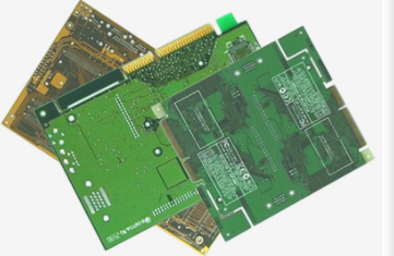
鑫景福致力于滿足“快速服務(wù),零缺陷,輔助研發(fā)”P(pán)CBA訂購(gòu)單需求。


PCBA方案設(shè)計(jì)
We often encounter various problems in PCB design, whICh is often a headache. Here are some common questions about PCB design skills
Ten common problems in PCB design
1. How to select PCB board?
The selection of PCB board must achieve a balance between meeting the design requirements and mass production and cost. The design requirements include electrical and mechanical parts. This material problem is usually important when designing very high-speed PCB boards (frequencies greater than GHz). For example, the commonly used FR-4 material has a dielectric loss at several GHz frequencies, which will greatly affect the signal attenuation, and may not be suitable. As far as electricity is concerned, pay attention to whether the dielectric constant and the dielectric loss are applicable at the designed frequency.

2. How to avoid high-frequency interference?
The basic idea to avoid high-frequency interference is to minimize the interference of high-frequency signal electromagnetic field, which is calLED crosstalk. You can increase the distance between high-speed signal and analog signal, or add ground guard/hunt traces beside analog signal. Attention should also be paid to the noise interference of digital ground to analog ground.
3. How to solve the problem of signal integrity in high-speed design?
Signal integrity is basically a problem of impedance matching. The factors that affect impedance matching include the structure of the signal source and output impedance, the characteristic impedance of the routing, the characteristics of the load side, and the topology architecture of the routing. The solution is to terminate and adjust the topology of routing.
4. How is the difference distribution line realized?
Two points should be noted in the wiring of differential pairs. One is that the length of the two lines should be the same as far as possible, and the other is that the distance between the two lines (which is determined by the differential impedance) should always remain unchanged, that is, they should remain parallel. There are two parallel ways. One is that two lines walk on the same side by side, and the other is that two lines walk on the upper and lower adjacent layers. Generally, the former has many side by side implementations.
5. For the clock signal line with only one output terminal, how to realize the difference distribution line?
It is meaningful to use differential distribution lines only if both the signal source and the receiver are differential signals. Therefore, the difference distribution line cannot be used for the clock signal with only one output terminal.
6. Can a matching resistance be added between differential line pairs at the receiving end?
The matching resistance between differential line pairs at the receiving end is usually added, and its value should be equal to the value of differential impedance. This will improve the signal quality.
7. Why should the wiring of differential pairs be close and parallel?
The wiring of differential pairs should be properly close and parallel. The so-called appropriate approach is because this distance will affect the value of differential impedance, which is an important parameter for designing differential pairs. The need for parallelism is also due to the need to maintain the consistency of differential impedance. If the two lines are either far or near, the differential impedance will be inconsistent, which will affect signal integrity and timing delay.
8. How to deal with some theoretical conflicts in actual wiring?
1. Basically, it is right to divide and isolate the analog/digital signal. It should be noted that the signal wiring should not cross the moit, and the return current path of the power supply and signal should not become too large.
2. The crystal oscillator is an analog positive feedback oscillation circuit. If there is a stable oscillation signal, it must meet the specifications of loop gain and phase. The oscillation specifications of this analog signal are very easy to be interfered. Even if ground guard traces are added, it may not be able to completely isolate the interference. Moreover, if it is too far away, the noise on the ground plane will also affect the positive feedback oscillation circuit. Therefore, the distance between the crystal oscillator and the chip must be as close as possible.
3. It is true that there are many conflicts between high-speed cabling and EMI requirements. However, the basic principle is that some electrical characteristics of the signal cannot meet the specifications due to the resistance capacitance or ferrite beam added by EMI. Therefore, it is better to solve or reduce the EMI problem by using the techniques of routing and PCB stacking, such as high-speed signal routing to the inner layer. Finally, use resistance capacitor or ferrite beam to reduce the damage to the signal.
9. How to solve the contradiction between manual wiring and automatic wiring of high-speed signals?
Most automatic routing devices with strong routing software now have set constraints to control the winding mode and the number of vias. The setting items of winding engine capacity and constraints of various EDA companies are sometiMES far from each other. For example, whether there are enough constraints to control the way of serpentine winding, and whether the distance between differential pairs can be controlled. This will affect whether the routing method of automatic routing can conform to the designer's idea. In addition, the difficulty of manually adjusting the wiring is also absolutely related to the ability of the winding engine. For example, the pushing ability of routing, the pushing ability of vias, and even the pushing ability of routing to copper coating, etc. Therefore, the solution is to choose a router with strong winding engine.
10. About test coupling.
The test coupler is used to measure whether the characteristic impedance of the PCB produced meets the design requirements with TDR (Time Domain Reflectometer). Generally, the impedance to be controlled includes single wire and differential pair. Therefore, the routing line width and line spacing (when there is differential alignment) on the test coupler should be the same as the lines to be controlled. The most important is the position of the grounding point during the measurement. In order to reduce the inductance of the ground lead, the place where the TDR probe is grounded is usually very close to the place where the signal is measured. Therefore, the distance and method between the measuring signal point on the test coupler and the grounding point should conform to the probe used.


抖音二維碼

Q Q二維碼

微信二維碼
點(diǎn)擊
然后
聯(lián)系
然后
聯(lián)系
電話熱線
13410863085Q Q

微信

- 郵箱