鑫景福致力于滿足“快速服務,零缺陷,輔助研發”PCBA訂購單需求。


PCBA方案設計
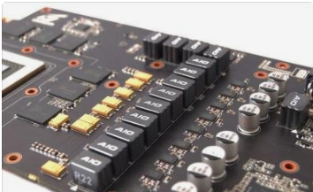
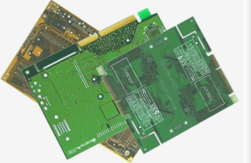
The core part of the PCBA finished product is the PCB, and the most basIC part of the PCB is the circuit. Next, we will introduce the schematic diagram of PCB design wiring rules and the analysis of PCB design wiring reference factors. PCBA cloning processing and PCBA development processing are essential for the understanding of PCB wiring.
Basic rules for PCB wiring
1、 Control the routing direction
The wires at the input and output terminals shall not be parallel to each other. During PCB wiring, the routing directions of adjacent layers are orthogonal, so as to avoid routing different signal lines in the same direction in adjacent layers, so as to reduce unnecessary inter layer interference. Signal crosstalk has a great impact on the function of PCBA processed products. When PCB wiring is restricted by structure (such as some backplanes) and it is difficult to avoid parallel wiring, especially when the signal rate is high, consider isolating each wiring layer with ground plane and isolating each signal line with ground wire

2、 Check open loop and closed loop of wiring
In PCB wiring, in order to avoid the "antenna effect" generated by wiring and reduce unnecessary interference radiation and reception, it is generally not allowed to have a wiring form with one end floating, otherwise unpredictable results may be brought to PCBA processing.
3、 Control the length of routing
1. Keep the routing length as short as possible
During PCB wiring, the routing length should be as short as possible to reduce the interference caused by the routing length
2. Adjust the routing length
PCBA processing has strict requirements on timing. In order to meet the requirements of signal timing, adjusting the signal routing length on PCB has become a part of PCB design.
4、 Control the length of routing branch
During PCB wiring, try to control the length of the routing branch to make the length of the branch as short as possible. In addition, it is generally required that the routing delay tdelay ≤ trise/20, where trise is the rise time of the digital signal. Schematic Diagram for Length Control of Routing Branch
5、 Corner design
During PCB wiring, routing turns are inevitable. When routing turns at right angles, additional parasitic capacitance and inductance will be generated at the corners. The corners of routing turns should not be designed as acute angles and right angles to avoid unnecessary radiation and affect the performance of PCBA processing products. At the same time, the process performance of acute angle and right angle is also poor. It is required that the included angle between all lines should be greater than or equal to 135 °. In the case that right angle corners are really needed for wiring, two improvement methods can be adopted: one is to change 90 ° corners into two 45 ° corners; The other is to use round corners. The round corner method is the best, and the 45 ° corner can be used at 10GHz frequency. For 45 ° corner routing, the corner length should be L ≥ 3W
6、 Differential pair routing
In order to avoid the impact of an imperfect return path, differential pair routing can be used. In order to obtain better signal integrity, differential pair routing can be used to realize high-speed signal transmission. The LVDS level transmission described above uses the differential transmission line.
1. Advantages of differential signal transmission:
a. The total di/dt of output drive will be greatly reduced, thus reducing the track collapse and potential electromagnetic interference.
b. The differential amplifier in the receiver has a higher gain than the single ended amplifier.
c. When differential signals are transmitted in a tight coupLED differential pair, they are more robust against crosstalk and mutation in the return path.
d. Because each signal has its own return path, the differential signal is not vulnerable to switching noise when passing through the connector or package.
2. Disadvantages of differential signal:
a. If the differential signal is not properly balanced or filtered, or if there is any common mode signal, EMI problems may occur.
b. Compared with single ended signal, the transmission of differential signal requires double signal lines.
3. The following principles shall be followed when designing differential pair routing.
a. Keep the distance S between the two signal routes of the differential pair constant throughout the route.
b. Ensure D > 2S to minimize crosstalk between two differential pair signals.
c. Make the distance S between the two signal lines of the differential pair meet S=3H, so as to minimize the reflection impedance of the element.
d. Keep the length of the two differential signal lines equal to eliminate the phase difference of the signal.
e. Avoid using multiple vias on differential pairs, as vias can cause impedance miSMAtch and inductance.
7、 Impedance of control PCB wire and matching of wiring terminal
In high-speed digital Circuit PCBA processing and RF circuit PCBA processing, there are requirements for the impedance of PCB wires, and the impedance of PCB wires needs to be controlled. During PCB wiring, the line width of the same network shall be consistent. Because the change of line width will cause the nonuniform characteristic impedance of the line, which will reflect the signal transmitted by the high-speed digital circuit, this situation should be avoided as far as possible in the design. Under certain conditions, such as connector outlet, BGA encapsulated outlet and other SIMilar structures, if the line width cannot be avoided, the effective length of the inconsistent part in the middle should be controlled and reduced as much as possible.
In high-speed digital circuits, when the delay time of PCB wiring is greater than 1/4 of the signal rise time (or fall time), the wiring can be regarded as a transmission line. In order to ensure the correct matching between the input and output impedance of the signal and the impedance of the transmission line, a variety of terminal matching methods can be used. The selected matching method is related to the connection mode of the network and the topology of the wiring.
8、 Design grounding protection wiring
In the PCB design of analog circuits, protective routing is widely used. For example, in a two-layer board without a complete ground plane, if both sides of the routing of a sensitive audio input circuit walk a grounding routing, crosstalk can be reduced by an order of magnitude.
In the digital circuit, a complete grounding plane can be used to replace the grounding protection wiring. The grounding protection wiring has more advantages than the complete grounding plane in many places.
According to experience, if a third wire with both ends grounded is inserted between two microstrip lines, the coupling between the two microstrip lines will be halved. If the third wire is connected to the ground plane through many through holes, their coupling will be further reduced. If there is more than one ground plane layer, it is necessary to ground at both ends of each protective route, not in the middle.
9、 Prevent wiring resonance
During PCB wiring, the wiring length shall not be an integral multiple of its wave length to avoid resonance.
10、 Some process requirements for wiring
1. Wiring scope
The size requirements of the wiring scope are shown in the table, including the size of the inner and outer layers of lines, copper foil to the board edge, and nonmetallic hole wall.
2. Line width and line spacing of wiring
If the PCBA assembly processing density permits, the lower density wiring design shall be selected as far as possible to improve the manufacturing capability of defect free and reliability. At present, the processing capacity of general manufacturers is: the minimum line width is 0.127mm (5mil), and the minimum line spacing is 0.127mm (5mil).
3. Connection between wire and chip component pad
When connecting wires and chip components, they can be connected at any point in principle. However, the chip components welded by reflow welding should be designed according to the following principles.
a. For components installed with two bonding pads, such as resistance and capacitance, the printed wire connected with the bonding pad should be symmetrically led out from the center of the bonding pad, and the printed wire connected with the bonding pad must have the same width. This provision can be ignored for outgoing lines with a line width less than 0.3mm (12mil).
b. The bonding pad connected to the wider printed wire should preferably be transited through a narrow printed wire in the middle, which is usually called the "heat insulation path". Otherwise, the 2125 (inch system, i.e. 0805) and the following SMDs are prone to "vertical" defects during welding.
4. Wire connection with bonding pad of SOIC, PLCC, QFP, SOT and other devices
When connecting the line to the bonding pad of SOIC, PLCC, QFP, SOT and other devices, it is generally recommended to lead the wire out from both ends of the bonding pad
3、 Decoupling capacitor configuration
Power input terminal jumper 10~100 μ F electrolytic capacitor. If possible, connect to 100 μ F is better.
In principle, each integrated circuit chip should be equipped with a 0.01pF ceramIC chip capacitor. If the gap between printed boards is insufficient, a 1-10pF tantalum capacitor can be arranged every 4-8 chips.
For components with weak noise resistance and large power change during power off, such as RAM and ROM storage components, decoupling capacitors should be connected between the power line and ground wire of the chip.
The capacitor lead shall not be too long, especially the high-frequency bypass capacitor shall not have lead.
If there are contactors, relays, buttons and other components in the printed circuit board, large spark discharge will occur when they are operated. RC circuit must be used to absorb the discharge current. Generally, R is 1~2k Ω, C is 2.2~47 μ F。
CMOS has a high input impedance and is susceptible to induction, so the unused ports should be grounded or connected to a positive power supply when in use.
4、 Wiring between components
No cross circuit is allowed in PCB printed circuit. For lines that may cross, "drilling" and "winding" can be used to solve the problem.
The grounding point of the circuit at the same level shall be as close as possible, and the power filter capacitor of the circuit at this level shall also be connected to the grounding point at this level.
The general ground wire must be arranged in the order of "weak current to strong current" step by step in strict accordance with the principle of "high frequency medium frequency low frequency", and it is not allowed to randomly turn over and over.
When using the IC base, pay special attention to whether the positioning slot on the IC base is placed in the correct direction, and whether the positions of each IC pin are correct.
This article mainly introduces the schematic diagram of PCB design wiring rules and the analysis of PCB design wiring reference factors


抖音二維碼

Q Q二維碼

微信二維碼
點擊
然后
聯系
然后
聯系
電話熱線
13410863085Q Q

微信

- 郵箱