鑫景福致力于滿足“快速服務,零缺陷,輔助研發”PCBA訂購單需求。


PCBA方案設計
Explain the capacitance of PCB design?
The structure and characteristICs of capacitors designed by potential are applicable to conductors, which are charged However, at the same potential, the amount of charge contained in the conductor varies with its own structure The ability of a conductor to retain charge is calLED the capacitive PCB design of the conductor Normally, the charge Q (Coulomb) in a conductor is productive to its potential V (Volt, relative to the earth), that is, it exists, and C is the capacitive PCB design of the conductor Capacitive tissue PCB design is Farah (F)
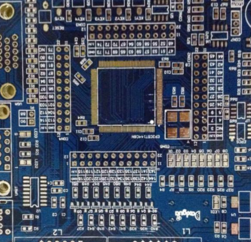
chip processing plant
The insulating medium is inserted between two parallel metal plates, and the wire electrode becoMES a capacitor designed by PCB PCB design PCB is based on circuit schematic diagram to achieve the functions required by circuit designers The design of printed circuit board mainly refers to layout design, which needs to consider the layout of external connections The circuit symbols are polar capacitance PCB design and non-polar capacitance PCB design If the PCB design is charged, the charge will accumulate on the bipolar plate of the capacitor Capacitors designed for PCB with capacitance C are represented by constant current intensity I Assume that the PCB design is not charged initially, that is, the initial voltage at both ends of the capacitor is equal to zero We remember the definition of current: the amount of charge passing through the conductor cross section in the organization time is called current intensity, that is, it exists because it is located in the PCB design
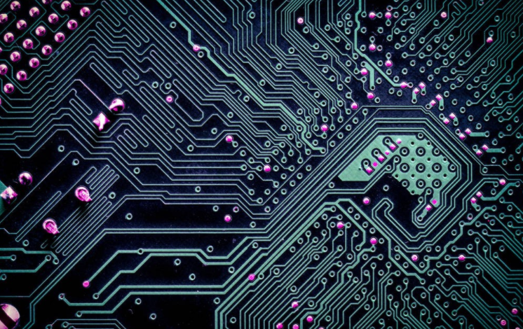
Circuit board

Therefore, the amount of charge flowing through the cross-section of the conductor during tissue time is called current intensity It is the current intensity
It is the capacitance designed by PCB and the capacitance designed by PCB C. Under the action of constant current intensity I, the voltage V at both ends increases linearly with time. The higher the voltage at both ends of a PCB designed capacitor, the more charges it contains and the greater the energy storage. However, the resistance of the insulating medium between the two boards of the capacitor designed by PCB is limited. If the electric field strength between the two boards is too high, the insulation medium may break down and the capacitor designed by PCB will be short circuited. In practical application, it is necessary to coordinate the voltage and resistance of capacitors designed by PCB. Conclusion: The capacitor designed by PCB has the function of holding the charge in the circuit, that is, energy storage. The capacitor designed with PCB has a long energy storage time and cannot change the voltage at both ends of the capacitor designed with PCB. The larger the capacitance of PCB design, the more energy can be stored. The capacitance and voltage resistance of PCB design are the most important parameters in PCB design. 2. RC charging and discharging circuit is represented by RC charging and discharging circuit. Assume that the initial voltage at both ends of the PCB design capacitor is zero, switch K is connected to one end, and the power supply charges the PCB design capacitor through resistor R. The charging current of PCB design capacitor is the maximum E/R. If you continue to charge with this current, the rising curve of VC is a straight line. However, due to the charging current during the whole charging process, with the increase of VC, the charging current intensity IC gradually decreases, and the amplitude of VC gradually increases until it reaches the power supply voltage E, while the charging current is zero. This forms the actual VC rising curve. Vc rises exponentially, and its change with time t is expressed as
This is a time constant.
It can be seen that the larger the series resistance R, the SMAller the charging current and the longer the charging time; The larger the capacitance C of PCBA design, the greater the power required (i.e., the more energy stored), and the longer the charging time.
When the capacitor is overcharged by PCB board, VC is equal to E When the switch K is turned on, the discharge current of the capacitor designed by PCB decreases gradually after R discharge Optimized layout of internal electronIC components pcb design company, optimized layout of metal connection and through-hole, electromagnetic protection, heat dissipation and other factors, excellent layout design can save production costs and achieve good circuit efficiency and heat dissipation efficiency


抖音二維碼

Q Q二維碼

微信二維碼
點擊
然后
聯系
然后
聯系
電話熱線
13410863085Q Q

微信

- 郵箱