鑫景福致力于滿足“快速服務,零缺陷,輔助研發(fā)”PCBA訂購單需求。


PCBA方案設計
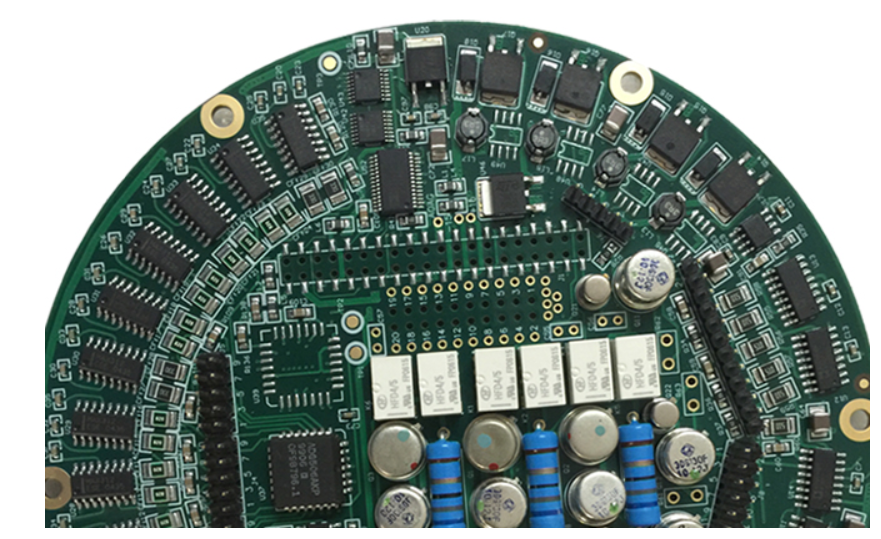
printed circuit board {PCB circuit board}, also known as printed circuit board, is the provider of electrICal connection of electronIC components. Its development has a history of more than 100 years; Its design is mainly layout design; The main advantage of using circuit board is to greatly reduce wiring and assembly errors, and improve the automation level and production labor rate.

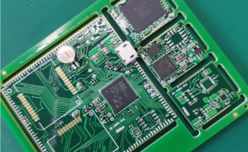
As PCB is not a general terminal product, the definition of its name is slightly confused. For example, the motherboard for personal computers is calLED the motherboard, but not the circuit board. Although there are circuit boards in the motherboard, they are not the same. Therefore, when evaluating the industry, they cannot be said to be the same. Another example: because there are integrated circuit parts loaded on the circuit board, the news media call it IC board, but in fact it is not the same as printed circuit board. The printed circuit board we usually refer to the bare board - that is, the circuit board without upper element devices.
PCB has developed from single-sided to double-sided, multi-layer, flexible and flexible, and still maintains its own development trend. Due to the continuous development towards high precision, high density and high reliability, and the continuous reduction of volume, cost and performance, printed boards will still maintain strong vitality in the future development of electronic equipment.
How is PCB designed? After reading the following seven steps, you will understand
1. Preliminary preparation
Including preparation of components and schematic diagrams. Before PCB design, first prepare schematic SCH components and PCB component packaging library.
The PCB component packaging library should preferably be established by engineers according to the standard size data of the selected components. In principle, the component packaging library of PC shall be established first, and then the schematic SCH component library shall be established.
PCB component packaging library has high requirements, which directly affects the installation of PCB; The schematic SCH component library is relatively loose, but pay attention to defining the pin attributes and the corresponding relationship with PCB component packaging library.
2. PCB structure design
According to the determined PCB size and various mechanical positioning, the PCB frame is drawn in the PCB design environment, and the required connectors, keys/switches, positioning holes, assembly holes, etc. are placed according to the positioning requirements.
Fully consider and determine the wiring area and non wiring area (such as how much area around the positioning hole belongs to the non wiring area).
Layout design is to place components in PCB frame according to design requirements. Generate the network table in the schematic tool (Design → Create Netlist), and then import the network table in the PCB software (Design → Import Netlist). After the network table is successfully imported, it will exist in the software background. Through the Placement operation, all devices can be called out, and there is a fly wire prompt connection between pins. At this time, the device layout can be designed.
PCB layout design is the first important process in the whole PCB design process. The more complex the PCB is, the better the layout will directly affect the difficulty of later wiring.
The layout design relies on the basic circuit skills and rich design experience of PCB designers, which is a high level requirement for PCB designers. The junior PCB designer has little experience and is suitable for SMAll module layout design or PCB layout design task with low difficulty.
4. PCB wiring design
PCB wiring design is the most workload process in the whole PCB design, which directly affects the performance of PCB.
During PCB design, there are generally three states of wiring:
The first is layout, which is the most basic entry requirement for PCB design;
The second is the satisfaction of electrical performance, which is the standard to measure whether a PCB board is qualified. After the wiring is completed, carefully adjust the wiring to achieve the best electrical performance;
Thirdly, the neat and beautiful, disorderly wiring, even if the electrical performance is qualified, will bring great inconvenience to the optimization, testing and maintenance of the later board modification. The wiring should be neat and uniform, and should not be crisscross and disorganized.
5. Wiring optimization and silk screen placement
"There is no best but better PCB design" and "PCB design is a defective art". This is mainly because PCB design aims to meet the design requirements of all aspects of hardware, while individual requirements may conflict, and you can't have both.
6. Network DRC check and structure check
Quality control is an important part of PCB design process. General quality control means include: design self inspection, design mutual inspection, expert review meeting, special inspection, etc.
Schematic diagram and structure element diagram are the most basIC design requirements. Network DRC inspection and structure inspection are to confirm that PCB design meets the two input conditions of schematic network table and structure element diagram respectively.
Generally, circuit board designers have their own accumulated design quality check lists. Some of the items come from the company's or department's specifications, and the other part coMES from their own experience. Special inspection includes design Valor inspection and DFM inspection, which focus on PCB design output back-end processing photo file.
7. PCB board making
Before the PCB is formally processed, the PCB designer needs to communicate with the PE of the PCB supplier and answer the manufacturer's confirmation questions about PCB processing.
This includes, but is not limited to, the selection of PCB plate models, the adjustment of line width and line spacing of circuit layers, the adjustment of impedance control, the adjustment of PCB stack thickness, surface treatment processing technology, aperture tolerance control and delivery standards.
This article mainly introduces how to design pcb circuit board from the seven steps of PCB production


抖音二維碼

Q Q二維碼

微信二維碼
點擊
然后
聯(lián)系
然后
聯(lián)系
電話熱線
13410863085Q Q

微信

- 郵箱