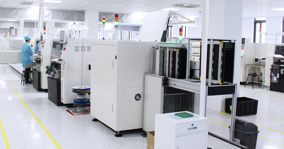
鑫景福致力于滿足“快速服務,零缺陷,輔助研發”PCBA訂購單需求。


PCBA方案設計
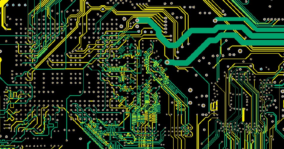
In any switching power supply design, the physICal design of the PCB board is the last link. If the design method is improper, the PCB may radiate too much electromagnetic interference, causing the power supply to work unstably. The following is an analysis of the matters needing attention in each step.
1. Design flow from schematic diagram to PCB
Create component parameters ->Input principle net list ->Design parameter setting ->Manual layout ->Manual routing ->Verify design ->Review ->CAM output.
2. Parameter Setting
The spacing between adjacent conductors must meet the electrical safety requirements, and in order to facilitate operation and production, the spacing should also be as wide as possible. The minimum spacing shall at least be suitable for the voltage. When the wiring density is low, the spacing of signal lines can be appropriately increased. The signal lines with high and low level differences shall be as short as possible and the spacing shall be increased. Generally, the wiring spacing is set to 8mil. The distance from the edge of the inner hole of the pad to the edge of the printed board shall be greater than 1mm, so as to avoid pad defects during processing. When the wiring connected with the pad is thin, the connection between the pad and the wiring should be designed as a water drop. This has the advantage that the pad is not easy to peel, but the wiring and the pad are not easy to disconnect.
Practice has proved that even if the circuit schematic is correctly designed and the printed circuit board is improperly designed, the reliability of electronic equipment will be adversely affected. For example, if two thin parallel lines of the printed board are close together, the delay of the signal waveform will be formed and the reflected noise will be formed at the end of the transmission line; The interference caused by improper consideration of power supply and ground wire will degrade the performance of the product. Therefore, correct methods should be used when designing printed circuit boards. Each switching power supply has four current circuits:
◆ AC circuit of power switch
◆ Output rectifier AC circuit
◆ Input signal source current circuit
◆ Output load current circuit Input circuit
The input capacitor is charged by an approximate DC current, and the filter capacitor mainly plays a broadband energy storage role; SIMilarly, the output filter capacitor is also used to store high-frequency energy from the output rectifier and eliminate the DC energy of the output load circuit. Therefore, the terminals of the input and output filter capacitors are very important. The input and output current circuits should be connected to the power supply only from the terminals of the filter capacitors; If the connection between the input/output circuit and the power switch/rectifier circuit cannot be directly connected to the terminal of the capacitor, the AC energy will be radiated to the environment by the input or output filter capacitor.
The AC circuit of the power switch and the AC circuit of the rectifier contain high amplitude trapezoidal currents. The harmonic component of these currents is very high, and its frequency is far greater than the basic frequency of the switch. The peak amplitude can be up to 5 tiMES the amplitude of the continuous input/output DC current. The transition time is usually about 50ns. These two circuits are most likely to generate electromagnetic interference, so these AC circuits must be laid before wiring other printed lines in the power supply. The three main components of each circuit, filter capacitor, power switch or rectifier, inductor or transformer, should be placed adjacent to each other. Adjust the component position to make the current path between them as short as possible.
The best way to establish the switching power supply layout is similar to its electrical design. The best design process is as follows:
1. Place the transformer
2. Design power switch current circuit
3. Design current circuit of output rectifier
4. Control circuit connected to AC power circuit
Design input current source circuit and input filter Design output load circuit and output filter According to the functional unit of the circuit, the layout of all components of the circuit shall comply with the following principles:
● PCB size shall be considered first. When the PCB size is too large, the printed line is long, the impedance increases, the noise resistance decreases, and the cost increases; If it is too SMAll, the heat dissipation is poor, and adjacent lines are vulnerable to interference. The best shape of the circuit board is rectangular, with a length to width ratio of 3:2 or 4:3. Components located at the edge of the circuit board are generally not less than 2mm from the edge of the circuit board
● When placing components, future welding shall be considered, not too intensive
● The core components of each functional circuit shall be taken as the center and arranged around it. The components shall be arranged evenly, orderly and compactly on the PCB, and the lead wires and connections between components shall be reduced and shortened as much as possible. The decoupling capacitor shall be close to the VCC of the components as much as possible
● For the circuit working at high frequency, the distribution parameters between components shall be considered. For general circuits, components shall be arranged in parallel as far as possible. In this way, it is not only beautiful, but also easy to assemble and weld, and easy to mass produce
● Arrange the position of each functional circuit unit according to the circuit flow, so that the layout is convenient for signal flow and the signal is kept in the same direction as far as possible
● The primary principle of layout is to ensure the distribution rate of wiring. Pay attention to the connection of flying wires when moving components, and put the components with wiring relationship together
● Reduce the loop area as much as possible to suppress the radiated interference of switching power supply
4. Wiring
The switching power supply contains high-frequency signals. Any printed wire on the PCB can act as an antenna. The length and width of the printed wire will affect its impedance and inductance, thus affecting the frequency response. Even the printed wire passing through the DC signal will be coupLED to the RF signal from the adjacent printed wire and cause circuit problems (or even radiate interference signals again). Therefore, all printed wires passing through AC current should be designed as short and wide as possible, which means that all components connected to the printed wire and other power lines must be placed close together.
The length of the printed wire is proportional to its inductance and impedance, while the width is inversely proportional to its inductance and impedance. The length reflects the wavelength of the printed wire response. The longer the length is, the lower the frequency of the printed wire that can send and receive electromagnetic waves, and it can radiate more RF energy. According to the current of the printed circuit board, try to rent the width of the power line to reduce the loop resistance. At the same time, make the direction of the power line and ground wire consistent with the direction of the current, which helps to enhance the anti noise ability. Grounding is the bottom branch of the four current loops of switching power supply, which plays an important role as the common reference point of the circuit and is an important method to control interference. Therefore, the placement of grounding wires should be carefully considered in the layout. Mixing various grounding wires will cause unstable power supply.
5. Inspection
After the wiring design is completed, it is necessary to carefully check whether the wiring design conforms to the rules formulated by the designer, and also to confirm whether the rules formulated conform to the requirements of the production process of printed boards. Generally, it is necessary to check whether the distances between lines, lines and component pads, lines and through holes, component pads and through holes, through holes and through holes are reasonable and meet the Production requirements. Whether the width of the power line and ground wire is appropriate, and whether there is a place in the PCB where the ground wire can be widened. Note: Some errors can be ignored. For example, some parts of the Outline of some connectors are placed outside the board frame, and errors will occur when checking the spacing; In addition, every time the routing and vias are modified, they should be copper coated again.
Recheck according to the "PCB checklist", including design rules, layer definition, line width, spacing, pad and via settings, and focus on the rationality of device layout, routing of power supply and ground wire networks, routing and shielding of high-speed clock networks, and placement and connection of decoupling capacitors.
6. Design output
Precautions for outputting photo files:
● The layers to be output include wiring layer (bottom layer), silk screen layer (including top layer silk screen, bottom layer silk screen), solder mask layer (bottom layer solder mask), drilling layer (bottom layer), and also generate drilling file (NC Drill)
● When setting the layer of silk screen layer, do not select the Part Type, but select the Outline, Text and Line of the top layer (bottom layer) and silk screen layer
● When setting the layer of each layer, select Board Outline. When setting the layer of silk screen layer, do not select Part Type, but select the outline, text and line of the top layer (bottom layer) and silk screen layer
● When generating drilling files, use the default settings of PowerPCB and do not make any changes


抖音二維碼

Q Q二維碼

微信二維碼
點擊
然后
聯系
然后
聯系
電話熱線
13410863085Q Q

微信

- 郵箱