鑫景福致力于滿足“快速服務,零缺陷,輔助研發”PCBA訂購單需求。


PCB制造
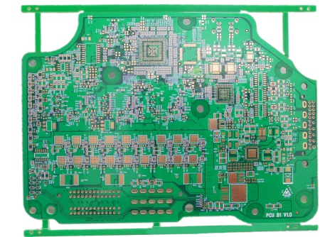
At present, the PCB manufacturing process of multilayer PCBs is mostly a subtraction method, that is, the excess copper foil on the raw material copper clad plate is subtracted to form a conductive pattern. The method of subtraction is chEMIcal corrosion, whICh is the most economical and efficient. Only the chemical corrosion has no differential attack, so it is necessary to protect the required conductive pattern. A layer of anti-corrosion agent should be coated on the conductive pattern, and then the unprotected copper foil corrosion should be subtracted. In the early days, the anti-corrosive ink was printed in line by screen printing, so it was calLED "printed circuit board". However, as electronic products become more and more sophisticated, the image resolution of printed circuits cannot meet the needs of products, and then photoresists are used as image analysis materials. The photoresist is a kind of photosensitive material, which is sensitive to the light source of a certain wavelength and forms a photochemical reaction with it to form a polymer. After the pattern is selectively exposed with a pattern negative, the unpolymerized photoresist is stripped through the developer (e.g. 1% sodium carbonate solution) to form a pattern protective layer.

In the current multi-layer circuit board manufacturing process, there is also the interlayer conduction function that is realized through metallized holes, so the PCB manufacturing process also needs to carry out drilling operations, and metallized electroplating operations for holes, and finally achieve interlayer conduction.
The manufacturing process of Multilayer PCBs is briefly described as follows:
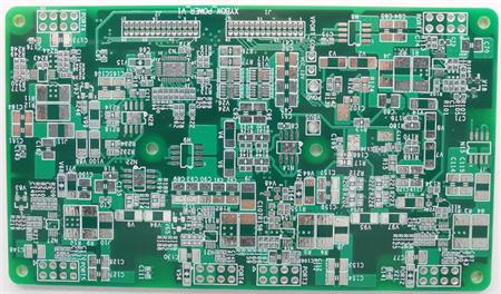
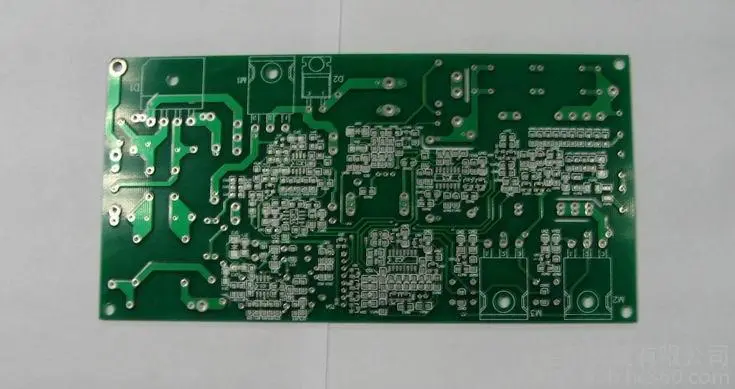
1、 First make two holeless double-sided boards
Blanking (raw material double-sided copper clad laminate) - inner layer pattern making (forming pattern anti-corrosive layer) - inner layer etching (minus excess copper foil)
2、 Glue and press the two prepared inner core plates with epoxy resin glass fiber prepreg
Rivet the two inner core plates with the semi cured sheet, then lay a copper foil on both sides of the outer layer and press it under high temperature and high pressure to make it stick together. The key material is the semi curing sheet, which has the same composition as the raw material. It is also epoxy resin glass fiber, but it is not fully cured and will liquefy at 7-80 ℃. Curing agent is added to it, which will react with the resin at 150 ℃
The crosslinking reaction is cured, and then it is no longer reversible. Through such a semi-solid liquid solid transformation, adhesion and bonding are completed under high pressure.
3、 Conventional double-sided board fabrication
Drilling - copper plate electricity (hole metallization) - outer circuit (forming a graphic anti-corrosive layer) - outer etching - solder resistance (printing green oil, text) - surface coating (tin spraying, gold deposition, etc.) - forming (milling forming).


抖音二維碼

Q Q二維碼

微信二維碼
點擊
然后
聯系
然后
聯系
電話熱線
13410863085Q Q

微信

- 郵箱