鑫景福致力于滿足“快速服務(wù),零缺陷,輔助研發(fā)”PCBA訂購單需求。


PCB制造
1. The impact of PCB layout/wiring on the electrICal performance is often seen in the books on electronics that "digital ground wire and analog ground wire should be separated". As everyone who has passed the board knows, this is difficult in practical operation.
To lay a better board, you must first have an electrical understanding of the IC you are using, which pins will generate high-order harmonics (the rising/falling edges of digital signals or switching value square wave signals), which pins are susceptible to electromagnetic interference, and the signal block diagram (signal processing unit block diagram) inside the IC will help us understand.
The overall layout is the primary condition to determine the electrical performance, while the layout between boards is more concerned with the direction or flow of signals/data between ICs. The general principle is that the part close to the power supply that is easy to generate electromagnetic radiation; The weak signal processing part is mostly determined by the overall structure of the equipment (i.e., the overall planning of the equipment in the early stage), and is as close to the input end of the signal or the detection head (probe) as possible, which can better improve the signal-to-noise ratio and provide more pure signals/accurate data for subsequent signal processing and data recognition.
2. PCB copper and platinum treatment
As the current IC working clock (digital IC) is getting higher and higher, its signal puts forward certain requirements for the width of the line. Wider lines (copper and platinum) are good for low frequency strong current, but not for high-frequency signals and data line signals. Data signals are more synchronous, and high-frequency signals are mostly affected by skin effect. Therefore, the two should be discussed separately.
High frequency signal wiring should be thin rather than wide, short rather than long, which also involves layout problems (signal coupling between devices), so as to reduce induced electromagnetic interference.
However, the data signal appears on the circuit in the form of pulse, and its high-order harmonic component is the decisive factor to ensure the correctness of the signal; The same wide copper and platinum will produce skin effect on high-speed data signals (the distributed capacitance/inductance will become larger), which will lead to signal deterioration and incorrect data identification. Moreover, if the line width of the data bus channel is inconsistent, it will affect the data synchronization problem (leading to inconsistent delay). In order to better control the synchronization problem of data signals, serpentine lines appear in the data bus routing, This is to make the signal in the data channel more consistent in delay. The large-area copper laying is aimed at shielding interference and inductive interference, and the double-sided board can give way to the ground as the copper layer; However, there is no problem of copper laying on multilayer boards, because the power supply layer between them plays a very good role in shielding and isolation.
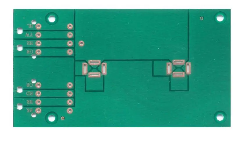
3. Layout between layers of Multilayer boards
Taking the four layer board as an example, the power supply (positive/negative) layer should be placed in the middle, and the signal layer should be routed in the outer two layers. Note that there should be no signal layer between the positive and negative power supply layers. The advantage of this approach is that the power supply layer plays the role of filtering/shielding/isolation as much as possible, while facilitating the production of PCB manufacturers to improve the yield.
4. Through hole
The engineering design shall minimize the design of vias, because vias are prone to generate electromagnetic radiation due to burrs while generating capacitance.
The hole diameter of the via should be SMAll and not large (this is for electrical performance; however, the too small hole diameter will increase the difficulty of PCB production, generally 0.5mm/0.8mm, 0.3mm should be used as small as possible). The probability of burrs occurring on small hole diameter after copper sinking process is smaller than that on large hole diameter, which is due to the drilling process.
5. Software application
Every software has its own ease of use, just your familiarity with the software. I have used PADS (power PCB)/PROTEL. When making SIMple circuits (familiar circuits), I will use PADS to directly layout; When making complex and new device circuits, it is better to draw the schematic diagram first and do it in the form of network table, which should be more correct and convenient.
There is no corresponding function to describe some non-circular holes in the software. My usual practice is to open a layer dedicated to expressing holes, and then draw the desired hole shape on this layer. Of course, the drawn wireframe should be filLED in. This is to better enable PCB manufacturers to identify their own expressions and explain them in the sample making instruction document.
6. PCB sent to manufacturer for sample preparation
1. PCB computer file
2. Layering scheme of PCB files (each electronic engineer's drawing habits are different, and PCB files after Layout will have different applications in layers, so you should attach a white oil diagram/green oil diagram/circuit diagram/mechanical structure diagram/auxiliary hole diagram of your files, and make a correct list document to explain your intentions)
3. PCB production prPCB production ocess requirements. You should attach a document to describe the process of making the board: gold plating/copper plating/tin spraying/rosin sweeping, board thickness specification, PCB board material (flame retardant/non flame retardant).
4. Number of samples
5. Of course, the contact information and responsible person should also be signed


抖音二維碼

Q Q二維碼

微信二維碼
點(diǎn)擊
然后
聯(lián)系
然后
聯(lián)系
電話熱線
13410863085Q Q

微信

- 郵箱