鑫景福致力于滿足“快速服務,零缺陷,輔助研發(fā)”PCBA訂購單需求。


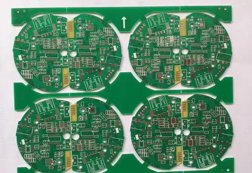
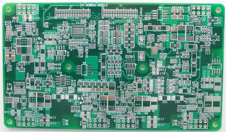
PCB制造
What are the defects of BGA welding
BGA welding is an important process in PCBA processing. However, because it is diffICult to inspect and maintain BGA after welding, X-ray fluoroscopy must be used to ensure the reliability of welding connection. Therefore, it is very important to diagnose BGA welding defects during reflow welding of pcba processing. Common BGA welding defects are described as follows.
BGA welding is an important process in PCBA processing. However, because it is difficult to inspect and maintain BGA after welding, X-ray fluoroscopy must be used to ensure the reliability of welding connection. Therefore, it is very important to diagnose BGA welding defects during reflow welding of PCBA processing.
Common BGA welding defects are described as follows.
(1) Blowing holes: holes or round pits appear on the surface of the solder ball.
Blowing diagnosis: During reflow soldering, there is gas overflow in the pores of BGA solder ball.
Blowing treatment: use X-Ray to check whether there are pores in the raw materials and adjust the temperature curve.
(2) Cold welding: the surface of the solder joint is not shiny and not completely welded.
Cold welding diagnosis: the welding spot is exposed due to insufficient heat and vibration during welding.
Cold welding treatment: adjust the temperature curve to reduce vibration during cooling.
What are the common BGA welding defects? How to handle
(3) Crystallization fracture: the surface of the solder joint shows glass crack.
Crystal fracture diagnosis: when gold is used as the welding pad, the crystal fracture occurs when gold and tin/lead are melted.
Crystal fracture treatment: tin is coated on the gold welding pad in advance, and the temperature curve is adjusted.
(4) Offset: BGA solder joint and PCB solder pad are misaligned.
Deviation diagnosis: the patch is inaccurate, and the conveying is vibrating.
Offset diagnosis: strengthen the maintenance of the placement machine, improve the placement accuracy, and reduce the vibration error.
(5) Bridging: Solder flows from the pad to another pad to form a bridge or short circuit.
Bridging diagnosis: solder paste and solder ball collapse, poor printing.
Bridging treatment: adjust the temperature curve, reduce the return air pressure, and improve the printing quality.
(6) Tin splashing: There is a SMAll tin ball near or between two solder joints on the PCB surface.
Tin splashing diagnosis: the quality of solder paste is poor and the temperature rises too fast.
Tin splashing treatment: check the storage time and conditions of solder paste, select appropriate solder paste as required, and adjust the temperature curve.
In the process of PCBa processing, correctly diagnose the BGA welding problems, and timely deal with them. It can not only reduce the loss caused by improper operation, but also detect the product quality from time to time.


抖音二維碼

Q Q二維碼

微信二維碼
點擊
然后
聯(lián)系
然后
聯(lián)系
電話熱線
13410863085Q Q

微信

- 郵箱