鑫景福致力于滿足“快速服務,零缺陷,輔助研發”PCBA訂購單需求。


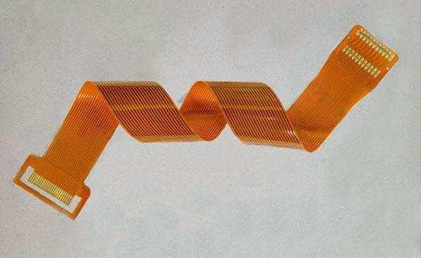
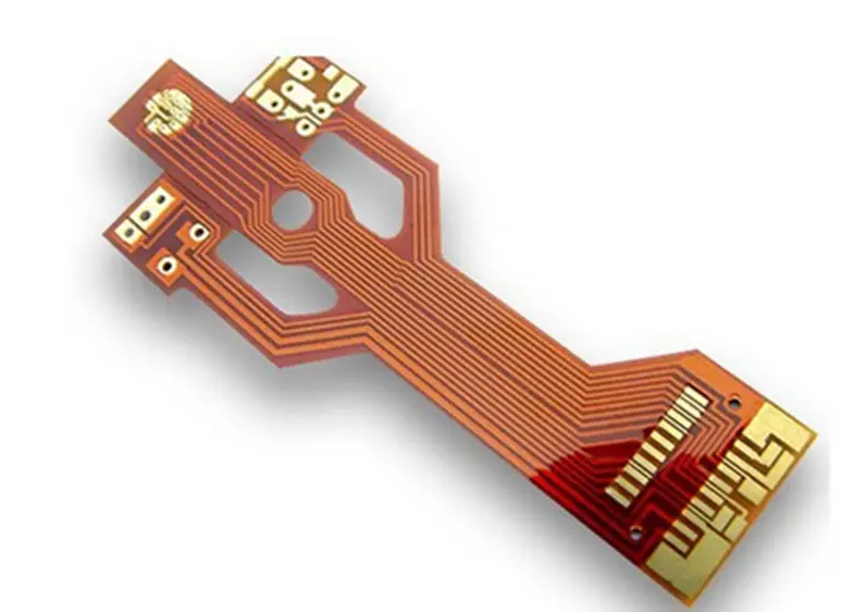
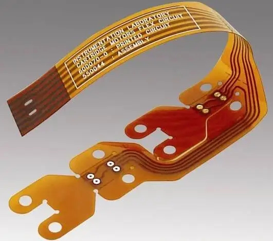
PCB制造
Circuit board board and surface treatment
Under the trend of "green electronICs", circuit board manufacturing will be impacted by many aspects. The new lead-free solder will lead to a sharp increase in reflow temperature and operation time, and the demand for heat resistance of substrate composition and downstream surface treatment such as solderability and printability; It will bring unprecedented new challenges to the process from inner layer treatment to finished plate surface treatment.
The requirement of halogen-free is a considerable challenge to the brevity of circuit board dielectric materials. Glass transition of sheet. The improvement of temperature (Tg) and the reduction of water absorption have become the important goals of the next generation of plates. This paper will provide a new solution to the artistic realm of RCF backed copper foil. Even for halogen-free HDI plates, it has been proved that they can show the best properties in practice.
The final surface treatment of the circuit board is closely related to the downstream lead-free assembly, and the various effects generated should be discussed in depth. In addition, the industry may give up the strong heat torture of lead-free tin spraying (HASL) and look for other alternatives, such as chEMIcal tin DIPping, chemical silver dipping, etc. This paper will also present the improvement results of new tin dipping, silver dipping and chemical nickel gold dipping in the past few years.
1、 Plate improvement
(1) Copper foil with adhesive backing
RCF or RCC backed copper foil has been widely used in mass production of micro blind holes for mobile phone circuit boards. The newly developed ruler RCC has greatly reduced the environmental hazards. The content of the material part can be divided into two parts: one is the change of the formula of the dielectric layer, and the other is the revolution of the manufacturing process of the adhesive backed copper foil itself. Ato decided to improve these two parts at the same time.
(2) The manufacturing process of friendly adhesive copper foil
At present, there are standard procedures for circuit board manufacturers to make adhesive backed copper foil. First, all components (resin, hardener, additive, flame retardant, etc.) are mixed and stirred in an organic solution, and then the fluid mixture is coated on the copper foil with a precision coater. Then, the solvent in the wet film is removed and dried in an oven.
Ato has developed a new solvent-free (So1Vent-1eSS) type backing copper foil: first, uniformly mix the solid raw materials, and then obtain an overall uniform powder through melt extrusion, so that no solvent is needed. In fact, this kind of manufacturing technology has already been applied in the field of decoration, and has also been very mature and widely used. In the new method, the original powder technology is used to uniformly coat the copper foil surface with a specific coating method, and then the improved system of the coating equipment is used to obtain a uniform powder layer. Then, the oven is gradually used to melt it under specific conditions, and after cooling, a uniform coating can be obtained on the copper foil. The skin film obtained by this method has a slightly rough appearance due to its SMAll fluidity, but it also allows the produced RCF to rapidly discharge gas in the subsequent pressing operation.
(3) Composition of halogen-free plates
In the past, the epoxy resin containing the odorous flame retardant has always been the main component of the base material plate, film, and back adhesive copper foil. However, since the EU legislation explicitly prohibits the application of certain toxic substances in electronic products, the industry has accelerated the replacement of such toxic substances. In the future, these toxic substances will no longer exist in the medium material formula.
The newly developed medium material of Ato is a halogen-free epoxy resin, which has passed the relevant halogen-free specifications. The formula uses phOSPhide as flame retardant and is changed into powder. In terms of material characteristics, it has not been sacrificed due to halogen-free. Especially in terms of key water absorption, it can still maintain a very low water content. The right table is an overview of various characteristics of odorless plates after pressing.
2、 Surface treatment and welding
This part mainly compares the wettability of various final surface treatments of circuit boards in general air or nitrogen. The surface treatments tested by Atoll include chemical tin, chemical silver, organic solder mask, lead-free tin spraying, medium and high phosphorus chemical nickel gold and nickel tin gold.
In order to clearly understand the best match between various surface treatments and lead-free soldering, the diameter of loose tin after solder paste melting should be measured after reflow. The plate used for the multi-function test board is FR4 of Tg170, with the thickness of 1.6mm and the thickness of copper plating on the surface of 30 μ m。
(1) . Layer Thickness
The most appropriate thickness range of lead-free welding is adopted for various surface treatments of the test welding, and the thickness of various coatings is carefully measured and verified in different ways.
(2) Reflow Soldering
The reflow soldering tried out by the Berlin Ato Head Office is a five section heated reflow soldering furnace of "REHM NITRO2100". The temperature time curve (Profile) used is the curve set according to J-STD-020-C. The maximum temperature of the board surface is 260 ℃, and the whole reflow soldering process does not exceed 10 minutes.
Each test welding is conducted in nitrogen environment (residual oxygen rate<100PPm) and general air environment (180KppmO2). The selected solder paste is SAC305 lead-free solder paste of "KOKI S3X58-M406". The solder paste is printed with stainless steel plate of "DEK248", the thickness of which is 125 μ m。


抖音二維碼

Q Q二維碼

微信二維碼
點擊
然后
聯系
然后
聯系
電話熱線
13410863085Q Q

微信

- 郵箱