鑫景福致力于滿足“快速服務,零缺陷,輔助研發”PCBA訂購單需求。


PCB制造
Reasons for circuit board delamination and its improvement
The Circuit board manufacturer and the circuit board designer explain the causes of circuit board layering and its improvement
As the European Union issued RoHS (Prohibition of the Use of Certain Hazardous Substances in ElectrICal and Electronic Equipment) and WEEE (Waste Electrical and Electronic Equipment) directives on February 13, 2003, the Circuit board assembly had to be lead-free. The lead containing tin was 63Sn/37Pb, and the melting point was 187 ℃ The composition of lead-free solder is SnAgCu (Sn96.5%/Ag3.0%/Cu0.5%), and the melting point is raised to 217 ℃. Then the corresponding welding temperature is raised from 220 ℃~ 230 ℃ to 240 ℃~ 260 ℃. The welding time that PCB must endure above the melting point is also extended by about 50 seconds. The probability of PCB being subjected to thermal shock is greatly increased. Therefore, the PCB must improve its heat resistance to match with it. With the gradual popularization of lead-free, the problem of circuit board layering has been puzzling circuit board practitioners.
Reasons for circuit board delamination: After the circuit board absorbs heat, different materials will have different expansion coefficients and form internal stress. If the adhesive force between resin and resin, resin and copper foil is not enough to resist this internal stress, delamination will occur, which is the fundamental reason for circuit board delamination. After lead-free, the extension of assembly temperature and time is more likely to cause circuit board delamination.
Improvement measures:
1. The base material shall be selected as qualified and reputable as possible, and the quality of PP material for Multilayer board is also a key parameter.
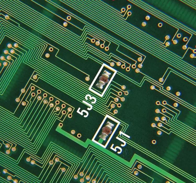
2. The lamination process is well controlLED, especially for multilayer boards with thick copper foil inside. As shown in the following figure, under the thermal shock, the inner layer of the multilayer board was delaminated, resulting in the scrapping of the whole batch.
3: Copper quality. The denser the copper layer on the inner wall of the hole is, the thicker the copper layer is, the stronger the thermal shock resistance of the circuit board is. Both the reliability of the circuit board is high and the production cost is low. Each step of the electroplating process control requires fine control.
When the circuit board is in the process of high temperature, the copper foil in the hole is broken due to the excessive expansion of the board. This means that the vias are blocked. This is also a precursor of stratification, which is manifested when the degree of stratification increases.
Conditional circuit board manufacturers have their own testing laboratories, which can observe the thermal shock resistance of their circuit boards in real time.
To sum up: circuit board layering is the result of a comprehensive situation. Only by making efforts in the selection of materials and process control, and keeping up with detection methods, can losses be reduced.


抖音二維碼

Q Q二維碼

微信二維碼
點擊
然后
聯系
然后
聯系
電話熱線
13410863085Q Q

微信

- 郵箱