鑫景福致力于滿足“快速服務,零缺陷,輔助研發”PCBA訂購單需求。


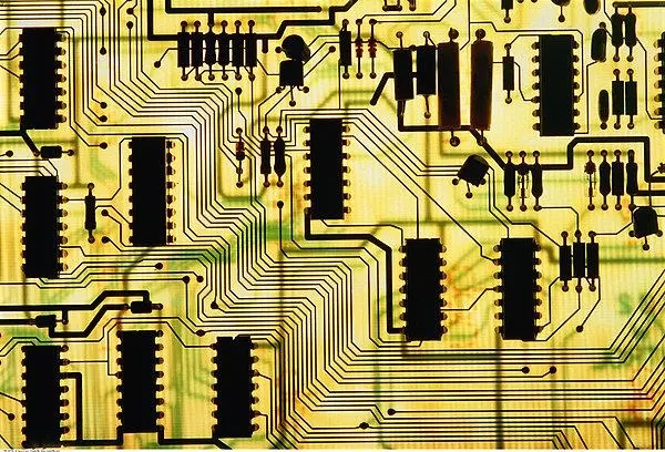
PCB制造
PCB process PCB printing process flow
In order to better enable customers to have a deeper understanding of the PCB manufacturing process, the PCB manufacturing process is described as follows: In electronic assembly, printed circuit boards are a key part. It carries other electronIC parts and connects circuits to provide a stable working environment for circuits. The circuit configuration can be divided into three categories:
[Single panel] The metal circuit providing part connection is arranged on the insulating substrate material, whICh is also the support carrier for installing parts.
[Double sided board] When the circuit on one side is not enough to provide the connection demand of electronic parts, the circuit can be arranged on both sides of the substrate, and a through hole circuit can be built on the board to connect the circuits on both sides of the board.
[Multilayer board] In case of complex application requirements, circuits can be arranged into multi-layer structures and pressed together, and through hole circuits can be arranged between layers to connect circuits of each layer.
The copper foil substrate of the inner layer circuit (only used for multilayer circuit board) shall be cut into a size suitable for processing and production. Before pressing the film on the substrate, it is usually necessary to roughen the copper foil on the plate surface with brush grinding, micro etching and other methods, and then attach the dry film photoresist to it with appropriate temperature and pressure. Send the substrate with the dry film photoresist to the ultraviolet exposure machine for exposure. The photoresist will polymerize after being exposed to ultraviolet light in the light transmission area of the negative film (the dry film in this area will be retained as an etching inhibitor in the later development and copper etching steps), and move the line image on the negative film to the dry film photoresist on the plate surface. After tearing off the protective adhesive film on the film surface, first develop and remove the areas on the film surface that are not exposed to light with sodium carbonate aqueous solution, and then use hydrochloric acid and hydrogen peroxide mixed solution to remove the exposed copper foil to form a circuit. Finally, use sodium hydroxide aqueous solution to wash the dry film which has been recovered. For the inner layer PCB with more than six layers (including), the riveting reference holes for the alignment of the inter layer circuits shall be punched by the automatic positioning punching machine.
Press fit (only for multilayer boards)
The finished inner circuit board must be bonded with the outer circuit copper foil with glass fiber resin film. Before pressing, the inner layer plate needs to be blackened (oxygenated) to passivate the copper surface and increase insulation; The copper surface of the inner circuit is roughened so as to produce good adhesion with the film. When stacking, first rivet the inner PCB with six layers of lines (including) or more in pairs with a rivet machine. Then put them neatly between the mirror steel plates in a container, and send them to the vacuum press to harden and bond the film with appropriate temperature and pressure. The pressed circuit board uses the X-ray automatic positioning drilling target machine to drill the target hole as the reference hole for the alignment of the inner and outer circuits. The plate edge shall be cut properly to facilitate subsequent processing.
Drilling
Use a CNC drilling machine to drill out the conductive holes of the interlayer circuit and the fixing holes of the welding parts on the circuit board. During drilling, the pin is used to fix the circuit board on the drilling machine table through the previously drilLED target hole. At the same time, a flat lower backing plate (phenolic resin plate or wood pulp plate) and an upper cover plate (aluminum plate) are added to reduce the occurrence of drilling burrs.
The primary copper of plated through-hole shall be coated with metallic copper layer after the forming of the interlayer conductive channel to complete the conduction of the interlayer circuit. First, clean the burrs on the hole and the dust in the hole by heavy brushing and high-pressure flushing, and then remove the glue residue on the copper surface of the hole wall with potassium permanganate solution. Soak and attach tin palladium colloid layer on the cleaned hole wall, and then reduce it to metal palladium. The circuit board is immersed in a chEMIcal copper solution, and the copper ions in the solution are reduced and deposited on the hole wall by the catalysis of palladium metal to form a through hole circuit. Then, the copper layer in the through hole is thickened by copper sulfate bath electroplating to be thick enough to resist the impact of subsequent processing and use environment.
Secondary copper of outer circuit
The production of line image transfer is like the inner line, but the line etching is divided into positive and negative production methods. The production method of the negative film is like the production of the inner circuit, which is completed by directly etching copper and removing the film after development. The production method of positive film is to add secondary copper and tin lead plating after development (the tin lead in this area will be retained as an etching inhibitor in the later copper etching step). After removing the film, the exposed copper foil will be corroded and removed with alkaline ammonia water and copper chloride mixed solution to form a line. Finally, the tin lead layer that has been retired will be stripped with the tin lead stripping solution (in the early days, the tin lead layer was retained and used to cover the line as a protective layer after being remelted, which is not used now).
Anti welding green paint
After the completion of the outer circuit, it is necessary to cover the insulated resin layer to protect the circuit from oxidation and welding short circuit. Before painting, it is usually necessary to roughen and clean the copper surface of circuit board by brush grinding, micro etching and other methods. Then, the liquid photosensitive green paint is applied to the board surface by screen printing, curtain coating, electrostatic spraying, etc., and then pre dried (the dry film photosensitive green paint is pressed and coated on the board surface by a vacuum laminator). After it cools down, it is sent to the ultraviolet exposure machine for exposure. The green paint will polymerize when it is exposed to ultraviolet light in the transparent area of the negative film (the green paint in this area will be retained in the later development step), and the areas that are not exposed to light on the film will be developed and removed with sodium carbonate aqueous solution. Finally, the resin in the green paint is completely hardened by baking at high temperature. The earlier green paint was produced by directly baking (or ultraviolet radiation) after screen printing to harden the paint film. However, in the process of printing and hardening, green paint often penetrates into the copper surface of the terminal contact of the line, causing problems in the welding and use of parts. Now, in addition to the use of SIMple and rough circuit boards, light sensitive green paint is mostly used for production.
Text printing
The text, tradeMARK or part number required by the customer is printed on the board by screen printing, and then the text paint is hardened by heating (or ultraviolet radiation).
Contact processing
Solder proof green paint covers most of the copper surface of the circuit, and only the terminal contacts for parts welding, electrical testing and circuit board plugging are exposed. This end point needs to be additionally provided with a proper protective layer to avoid oxide generation at the end point connecting the anode (+) during long-term use, which will affect the stability of the circuit and cause safety concerns.
[Gold plating] A layer of nickel layer with high hardness and wear resistance and gold layer with high chemical passivity shall be plated on the insertion terminal of the circuit board (commonly known as the golden finger) to protect the terminal and provide good connection performance.
[Tin spraying] Cover a layer of tin lead alloy on the welding end point of the circuit board with hot air leveling to protect the end point of the circuit board and provide good welding performance.
[Pre welding] Apply a layer of anti-oxidation pre welding coating on the welding end point of the circuit board in a DIP manner, temporarily protect the welding end point and provide a flat welding surface before welding, so as to have good welding performance.
[Carbon ink] A layer of carbon ink is printed on the contact end point of the circuit board by screen printing to protect the end point and provide good connection performance.
Forming and cutting
Cut the circuit board into the external dimensions required by customers with CNC molding machine (or die punch). When cutting, use the pin to fix the circuit board on the bed (or mold) through the previously drilled positioning hole for forming. After cutting, the golden finger shall be chamfered to facilitate the insertion and use of the circuit board. For multi chip molded circuit boards, more X-shaped break lines need to be added to facilitate customers to split and disassemble after plug-in. Finally, clean the powder on the circuit board and the ionic pollutants on the surface.
Final inspection package
Before packaging, conduct the final electrical conductivity, impedance test, solderability and thermal shock resistance test on the circuit board. The moisture absorbed by the circuit board in the manufacturing process and the accumulated thermal stress are eliminated by proper baking, and then the vacuum bag is used for packaging and shipping.


抖音二維碼

Q Q二維碼

微信二維碼
點擊
然后
聯系
然后
聯系
電話熱線
13410863085Q Q

微信

- 郵箱