鑫景福致力于滿足“快速服務,零缺陷,輔助研發”PCBA訂購單需求。


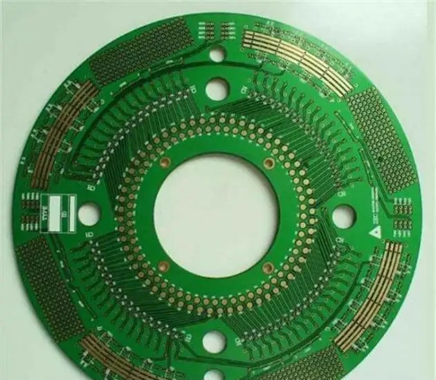
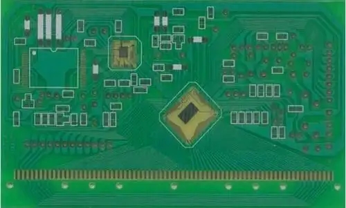
PCB制造
PCB Process COB Process Introduction_ Precautions_ Part I
COB (Chip On Board) is not a new technology in the electronIC manufacturing industry, but recently I have often been asked about relevant questions and data requests. Maybe the products are getting SMAller and smaller, and advanced technology is too expensive, so some people turn back to consider the COB process.
Here I reorganize the experience of COB erection and operation many years ago. On the one hand, I rEMInd myself of this process, and on the other hand, I provide reference. Of course, some information may not be up to date, and it is only for reference.
Evolution history of IC, COB, and Flip chip (COG)
The following figure shows the evolution history of electronIC chip packaging, from IC packaging to COB to Flip Chip (COG), which is becoming smaller and smaller. Among them, COB can only be said to be an intermediate product between current technologies.
COB is to directly paste the bare wafer on the circuit board (PCB), and directly solder the wire/wire on the gold plated circuit of the PCB, and then effectively transfer the packaging steps in the IC manufacturing process to the circuit board for direct assembly through the sealant technology.
In the past, COB technology was generally applied to consumer electronic products that didn't pay much attention to reliability, such as toys, calculators, small displays, clocks and watches, and other daily necessities, because most of the manufacturers who made COB were due to low cost considerations. Nowadays, more and more manufacturers are interested in its small size, as well as the trend of thin and short products. There is a growing trend in its application, such as mobile phones, CAMeras and other products that require short size.
COB has another advantage, which makes some PCBA manufacturers love it very much. Due to the need for sealant, the general COB will seal all external wire pins in epoxy resin. Hackers who like to crack other people's designs may spend more time to crack because of this feature, which indirectly improves the security level of anti hacking. (※: Anti hacking security level is determined by the amount of time spent to crack a technology)
COB Environmental Requirements
It is recommended to have a clean room and the class should be below 100K. Because the COB manufacturing process belongs to the wafer packaging level, any small particles contaminating the solder joint will cause serious defects.
The basic dust-free clothes and hats are also necessary. There is no need to wrap the pullover into a meat dumplings style dust-free clothes, but the basic hats, clothes, and static shoes are all necessary.
In addition, the clean room should strictly control the entry of cartons and any items that are easy to carry or produce wool. All packages should be unpacked outside the clean room before entering the clean room, which is to keep the clean room and extend the life of the clean room.
PCB design requirements of COB
1. The finished product surface treatment of PC board must be gold plated and a little thicker than the gold plating layer of general PC board to provide the energy required by Die Bonding and form gold aluminum or gold gold.
2. In the wiring position (layout) of the solder pad outside the Die Pad of COB, try to keep the length of each solder line fixed, that is, the distance between the solder joint from the die to the PCB solder pad should be as consistent as possible. Therefore, the design of welding pads with diagonal lines does not meet the requirements. It is suggested that the spacing of PCB pads can be shortened to eliminate the occurrence of diagonal pads.
3. It is recommended that a COB wafer should have at least two locating points. It is hoped that the traditional circular locating points will be replaced by the cross locating points, because the wire bonding machine will grasp the straight line for positioning when it makes automatic positioning again. Some Wire Bonding machine may be different. It is recommended to refer to the machine performance for design.
4. The size of the PCB (Die Pad) should be a little larger than the actual die to limit the offset when placing the wafer, but it should not be too large to avoid too serious rotation of the wafer. It is recommended that the wafer pad on each side is 0.25~0.3mm larger than the actual wafer.
5. The area where COB needs to be filLED with glue should not have layout through holes (vias). If it cannot be avoided, these through holes must be plugged 100% completely to prevent the epoxy glue from seeping through the other side of the PCB.


抖音二維碼

Q Q二維碼

微信二維碼
點擊
然后
聯系
然后
聯系
電話熱線
13410863085Q Q

微信

- 郵箱