鑫景福致力于滿足“快速服務,零缺陷,輔助研發(fā)”PCBA訂購單需求。


PCB制造
ClassifICation and Technology of High Density Circuit Boards
multilayer printed circuit board with one through hole electroplating
Through hole electroplating has been used for multilayer printed circuit boards for more than 20 years. To understand the circuit board industry, understanding through hole electroplating is a basic lesson for circuit board factories.
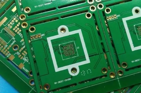
The through-hole of the circuit board generally provides two functions, namely, conducting the line between layers and installing through-hole components. If the through-hole is purely for conduction, there is a common saying in English calLED (Via), which is not exactly the same as the meaning of hole, but the Chinese word meaning is called hole, so there is a difference between the so-called part hole and the conduction hole. In order to improve the density of the circuit board, reduce the number of layers, and facilitate assembly, surface attached electronIC components are widely used. In addition to the large hole design for specific terminals and tool holes, almost all holes that are purely for general use are designed with the SMAllest hole as far as possible to reduce the occupied area.
Bimetal core plate and soft and hard plate
The circuit board designed for special purpose is different from the general multilayer circuit board, for example, the metal core Board Designed for high power consumption, high temperature and high heat equipment is an example.
The metal core plate places thicker metal in the area with high heating elements, and the power supply exposes the metal block directly to the elements. Some designs only use thicker copper skin to improve heat dissipation. Therefore, the thickness of common copper skin is about 0.5? 2 oz, its structure remains even. However, the metal core plate emphasizes the heat dissipation efficiency, and the commonly used metal thickness is about 3? 14oz, because a layer of thick metal is added, the total number of metal layers is often singular, which is very different from ordinary circuit boards. Although the complexity of metal core plate is considered in the fabrication procedure and design, it still has its value for high-power equipment and components.
The soft and hard boards made of hard boards and soft boards are mainly designed to meet the requirements of performance improvement, lightweight, space saving, etc. It can avoid the trouble of connector wiring, but the cost is high due to the trouble of production procedures. Except for military and aerOSPace applications, such circuit boards can be seen in general electronic products such as display modules.
III. High density laminated printed circuit board
The high-density laminated printed circuit board is a circuit board made by using the sequential construction process of the circuit layer and insulation layer, and the structure formed is shown in Figure 4. At the early stage of the development of high-density circuit boards, the designed structure is based on the resin without reinforcement material as the insulating substrate of the high-density layer. Therefore, the design method is based on the traditional hard board structure, and then the high-density circuit with pure resin is built on it. Of course, there are also some circuit boards that adopt different approaches and do not follow the structure with a thicker substrate in the middle. Such a structure is called core less technology, and ALIVH developed in Japan is classified as such technology.
Because the traditional circuit board structure is not easy to make tiny holes, some developers have made holes by image transfer, laser technology or other hole forming methods, which can save the configuration space of the copper pad, reserve more space to make winding easier, and because the insulation layer is thinner, the characteristic impedance and electromagnetic effect also have better performance.
High density printed circuit board with four transfer method
The definition of high-density refers to that more copper pads and connecting wires can be configured in the same plane space. Therefore, technologies that can make thin wires, small holes and high cumulative density can be classified as high-density circuit board technologies.
The program of high-density circuit board is made by transfer printing. Because the circuit of such circuit board technology almost depends on electroplating, as long as the image film can analyze the thin circuit, the production of thin circuit is not a problem. Moreover, because the line is embedded in the resin, the stability of the line has a stronger binding force and a more stable line width spacing than the general line manufacturing method. The circuit is embedded with resin to make the board surface smooth. It is not difficult to cover the solder stop paint of general circuit boards due to the high circuit. Repeated use of this technology can obtain fine lines, but how to make the pre formed lines accurately stack with the board lines is a big problem.
High Density Circuit Board Made by Transfer Printing
Steel plate ->Copper plating ->Image transfer ->Line ->Plating ->Pressing ->Nickel plating and conduction process
Fig. 5 Procedures for manufacturing high-density circuit boards by transfer printing method of general circuit board manufacturers
V. High density printed circuit board with conductive paste
The purpose of electroplating is to make a production procedure for the conduction between layers. However, some circuit board makers use conductive paste as the conductive connection between layers. Therefore, there are two more well-known circuit boards in the Japanese MARKet. They are ALIVH developed by Panasonic and B4t developed by Toshiba.
The circuit board structure is formed by laser drilling and filling conductive paste into the through hole, then laminated with copper foil stack, and then made into wires. If you want to increase the level, just repeat the previous steps. Because the through-hole design is flexible, ALIVH (Any Layer Inner Via Hole) is called the circuit board technology of this structure, and Panasonic is also famous for this circuit board technology in the industry.
The circuit board is made by using conductive paste to make bumps. It mainly uses the cone shaped cylinder formed after the conductive paste is hardened as a tool to penetrate the film, and completes the interlayer conduction through such procedures as bump formation, film puncture, hot pressing, etc., and then makes a circuit to complete the basic circuit board structure. If you want to form more circuit layers, just repeat the above procedure. Because this i: high-density circuit board adopts conductive bump technology, it is called B 2i t (Buried Bump Interconnection Technology). This technology does not limit the special film substrate, so the elasticity of material selection is larger than ALIVH.
Production of conductive paste
Lower copper sheet - "bump fabrication -" coating LCP insulating material - "upper copper sheet pressing -" circuit fabrication - "core plate 1+core plate 2 -" pressing
Size Planning and Control of Circuit Boards
11-01,2022


抖音二維碼

Q Q二維碼

微信二維碼
點擊
然后
聯(lián)系
然后
聯(lián)系
電話熱線
13410863085Q Q

微信

- 郵箱