鑫景福致力于滿足“快速服務,零缺陷,輔助研發”PCBA訂購單需求。


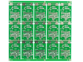
PCB制造
Size Planning and Control of Circuit Boards
Multilayer circuit board is a structural element composed of a dielectrIC layer and a circuit, and the circuit is arranged on the surface and inside of the dielectric material. Common size planning criteria must be available when designing, otherwise, most electronIC components on the MARKet cannot reach commonality. Such wiring design rules are the design rules of PCBA boards.
1 Grid
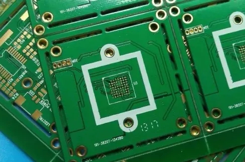
Because the positions of all components on the circuit board are relative coordinates, the original idea of circuit board configuration is to allocate blocks on the circuit board plane with imaginary grid lines. As the circuit board was first dominated by European and American countries, the early specifications were based on 1/10 inch, while the metric units were based on 2. 5 mm. The British system was equivalent to lOOmil. On this basis, subdivide the different spacing, and make the location configuration of holes and copper pads, which is the traditional design principle of through-hole components. However, after the popularity of SMT - Surface Mount Technology, it is unrealistic to configure holes on grid points. Although there are grid points in the design, the actual design is not limited by the grid points for a few moments. The holes are more and more conductive, and the blind and buried holes are more independent of the grid points.
The most influential part of such changes is electrical testing. Because the traditional electronic component contact is based on grid point design, the design of both drilling and welding points is based on grid point. Therefore, all circuit boards that follow the grid design can use the so-calLED universal tool for electrical testing, but the testing must move to a more dense contact form after the grid principle is broken. Therefore, SMAll quantities of products begin to use the so-called flying probe for testing, while mass production uses the dedicated tool for testing.
2 Line width spacing
Thin wire design has become an inevitable trend in the development of high-density circuit boards, but the design of thin wire must take into account the changes in resistance and characteristic impedance of thin wire. The size of the line spacing is subject to the insulation of the dielectric material. For organic materials, about 4 mils can be selected as the target value. Due to the product demand and the progress of manufacturing technology, products with a spacing of about 2mil or even smaller have also entered the practical application. In the face of further reducing the line spacing of semiconductor packaging boards, how to maintain the proper insulation has become a subject that must be worked hard. Fortunately, the operating voltage of most high-density packaging boards is also relatively low, which is fortunate.
There are through holes and blind buried holes in the structure. The holes buried in the plate are called interlaced holes IVH (Interstitial Via Hole) by some people. The utility model is a circuit board for connecting microporous layers after the inner layer plates with plated through holes are continuously pressed together. The fabrication of these microporous layers can play a space saving function only by using a small diameter design. Generally, mechanical drilling is more economical to produce an aperture larger than 8mil. Although there is a claim that products smaller than 4mil can be produced, the cost is too high to be practical.
Due to the limitation of mechanical aperture and production rate, the circuit board using the layer adding method will not only use microporous technology for surface holes, but also design smaller for the built-in through-hole to improve the density. The reduction of aperture greatly increases the degree of freedom of circuit configuration, which makes high-density multilayer circuit boards popular.
The number of layers of multilayer circuit board is mainly determined by the allowable wiring density. In the past, the majority of circuit boards were composed of four layers, which was mainly due to the need for electromagnetic shielding of signal lines, rather than the need for winding density. Due to the increased complexity of electronic components, the original winding density and hierarchical design can no longer meet the needs, so the level is gradually improved. However, as increasing the number of layers will increase the production cost, we want to reduce the number of layers as much as possible during the initial design. Therefore, if more micropores and fine wires are used, the element can still be formed in a limited number of layers. Piece connection. Even so, with the progress of sEMIconductor components, the overall number of layers of high-speed circuit boards is still rising.
In terms of circuit structure, as the overall power of electronic products continues to increase and the transmission rate continues to increase, many designs will require a higher line thickness but also a thinner line under the condition of limited space and maintaining the conductor cross-sectional area. There are also strict restrictions on the thickness control of the interlayer dielectric layer and its allowable error, so the configuration of the inner substrate and film will become very important. Generally, the pressing structure of circuit board will be designed symmetrically, which is to reduce the uneven stress. Multilayer board structure.
For products requiring strict electrical characteristics, the correct integration of characteristic impedance and the allowable tolerance of interlayer thickness between power supply and ground plane will become more stringent. Therefore, many production procedures are to make the key thickness layers with the base material first, while the less important layers are handed over to the film to complete. Because the base material has been hardened in advance, it can be made by selecting the base material that meets the specifications, so it can improve the yield and electrical performance.
When designing high-density multilayer circuit boards, the number of circuit layers shall be determined according to the winding density, and the wiring mode, inter layer thickness, and circuit width and thickness shall be determined according to the electrical characteristics. In order to prevent bending and warping, try to use symmetric pressing design. In general, the power supply and ground plane of high-density laminate are mostly located on the inner hard board, and the signal layer is made by the laminate circuit to integrate the impedance characteristics, but this rule may not be followed for higher level products.


抖音二維碼

Q Q二維碼

微信二維碼
點擊
然后
聯系
然后
聯系
電話熱線
13410863085Q Q

微信

- 郵箱