鑫景福致力于滿足“快速服務,零缺陷,輔助研發”PCBA訂購單需求。


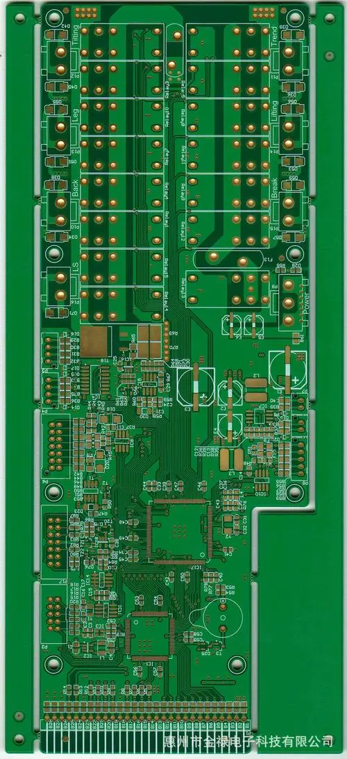
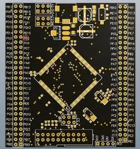
PCB制造
It has been said that there are only two kinds of electronIC engineers in the world: those who have experienced PCB electromagnetic interference in PCB design and those who have not experienced electromagnetic interference. With the increase of PCB routing express, EMC design is a problem that we electronic engineers have to consider. For a design, when conducting EMC analysis of a product and design, there are five important attributes to consider:
(1) Key device size: the physical size of the EMIssion device that generates radiation. Radio frequency (RF) current will generate electromagnetic field, which will leak through the enclosure and leave the enclosure. The routing length on the PCB as a transmission path has a direct impact on the RF current.
(2) Impedance matching: the impedance of the source and receiver, and the transmission impedance between them.
(3) Time characteristics of interference signal: whether this problem is a continuous (periodic signal) event or only exists in a specific operation cycle (for example, a single time may be a key operation or power on interference, periodic disk drive operation or network burst transmission).
(4) Intensity of interference signal: how strong is the source energy level, and how great is its potential to produce harmful interference.
(5) Frequency characteristics of interference signal: use the spectrometer to observe the waveform, and where the observed problem is in the spectrum, so as to find the problem.
In addition, some low frequency circuit design habits need attention. For example, my usual single point grounding is very suitable for low-frequency applications, but it was later found that it is not suitable for RF signal occasions, because there are more EMI problems in RF signal occasions. It is believed that some engineers apply single point grounding to the design of all PCB products without realizing that using this grounding method may cause more or more complex electromagnetic compatibility problems.
We should also pay attention to the current flow in the circuit components. With circuit knowLEDge, we know that the current flows from the place with high voltage to the place with low voltage, and the current always flows through one or more paths in a closed loop circuit, so a minimum loop and a very important law. For the direction in which the interference current is measured, modify the PCB routing so that it does not affect the load or sensitive circuit. For applications that require a high impedance path from the power supply to the load, all possible paths through which the return current can flow must be considered.
There is also a PCB wiring problem. The impedance of the conductor or wiring includes resistance R and inductive reactance. At high frequency, there is no capacitive reactance. When the wiring frequency is higher than 100kHz, the wire or wiring becoMES inductance. Wires or cabling that work above audio may become radio frequency antennas. In the EMC specification, it is not allowed for the wire or cable to run at a certain frequency λ/ Under 20 (the design length of the antenna is equal to that of a specific frequency λ/ 4 or λ/ 2) When the design is not careful, the cabling becomes a highly efficient antenna, which makes the later debugging more difficult.
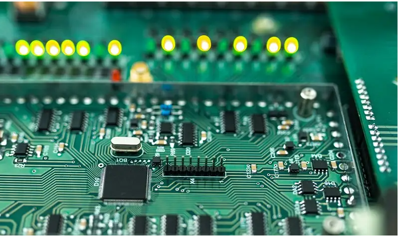
Finally, we will talk about PCB layout. First, consider PCB size. When the size of PCB is too large, the anti-interference ability of the system will decrease and the cost will increase with the increase of wiring, while the problem of heat dissipation and mutual interference will easily be caused when the size of PCB is too SMAll. Second, determine the position of special components (such as clock components) (the clock wiring should not be paved around and above or below the key signal lines to avoid interference). Thirdly, according to the circuit function, the overall layout of PCB is carried out. In terms of component layout, relevant PCB components should be as close as possible, so as to obtain better anti-interference effect.


抖音二維碼

Q Q二維碼

微信二維碼
點擊
然后
聯系
然后
聯系
電話熱線
13410863085Q Q

微信

- 郵箱