鑫景福致力于滿足“快速服務(wù),零缺陷,輔助研發(fā)”PCBA訂購單需求。


PCB制造
PCB circuit board sample is the most important step for any electronIC hardware design engineer and the beginning of all electronic products.
Pcb proofing
From PCB design to finished electronic products, gadgets, SMArt phones, home appliances or appliances, and so on, you can see all the electronic products and equipment. PCB board samples are very important. It allows testing of a given design to determine whether it is valid. This allows you to debug and correct any errors. This is also useful before mass production. If there is no PCB Prototype, the large-scale production of electronic circuit boards and related products still has risks.
In complex circuit boards, minor errors can be expensive and time-consuming and difficult to correct. Wrong design may make welding of electronIC components very difficult. It is also more difficult to point out the error points on the circuit board. Therefore, it is wise to design PCB sample proofing before actual production to avoid any future risks.
Now let's introduce what is a printed circuit board?
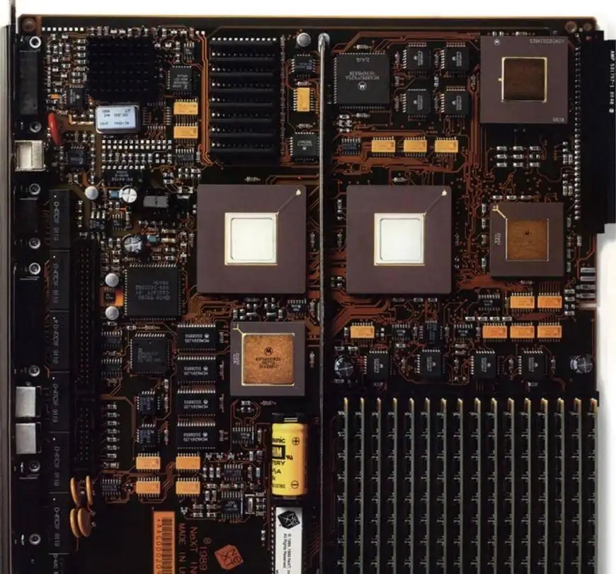
Most Electronic devices and products have PCB circuit boards. printed circuit board (PCB/PWB) is a board made of non insulating and highly heat-resistant insulating materials (such as glass fiber). These plates are also calLED baseplates. A PCB substrate can only have a single layer (single-layer circuit board) or more than one layer (multilayer circuit board). Conductive metals such as copper are used to make conductive paths or traces to promote current. Once PCB welding is completed, it is called "printed circuit board". After welding electronic components, the same PCB is called printed circuit board sEMI-finished product (PCBA).
pcb circuit board proofing
When designing a new circuit, it is very important to draw the schematic diagram of the circuit board before. The circuit board schematic will help debug and fix any errors that occur during this process. If the circuit on the circuit board is very SIMple, you can use a very simple sample board. In the case of complex and customized circuit boards, it is necessary to make sample PCB boards.
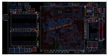
Design software of PCB circuit board layout
To start making PCB board samples, you need board making information such as Gerber files. PCB layout software can be used for this purpose. A circuit board layout software draws the layout of the circuit board and all traces, and points out that the electronic components will be soldered on the circuit board. The PCB layout looks like a diagram. The PCB layout software allows you to edit the layout until you achieve the desired layout.
How to make PCB
Manufacturing PCB involves several complex processes.
1: Film plate: In this process, mask or photomask is chemically etched to subtract copper area from PCB board substrate. Use CAD PCB software program to create photomask using photo plotter design. Photomasks are also created using a laser printer.
2: Lamination: multilayer PCB circuit boards are composed of multilayer thin etched boards or trace layers, and are bonded together through the lamination process.
3: Drilling: Each layer of PCB needs the ability to connect one layer to another; This is achieved by drilling a small hole called "VIAS". Drilling is mainly done by using automatic computer driven drilling machines.
4: Soldering pad tin spraying: the soldering points of electronic components are sprayed with tin or chemically deposited on the bonding pad on the PCB to facilitate the welding of electronic components. Bare copper is not easy to weld. It requires that the surface be plated with materials convenient for welding. Earlier lead based tin was used for plated surfaces, but with R oHS compliance, newer lead-free materials such as nickel and gold are now used for electroplating.
5: Testing PCB: Before soldering the PCB components to PCB, it is necessary to test them. This test can be performed with a test rack tester or a flying pin tester, which is a circuit board test equipment operated by other computers.
The manufacturing process and process procedures are similar for both PCB proofing and batch manufacturing, except that the cost of manufacturing PCB samples is different from the pre tooling cost allocated during batch manufacturing.
What are pcb board aging test aging test?
11-01,2022


抖音二維碼

Q Q二維碼

微信二維碼
點擊
然后
聯(lián)系
然后
聯(lián)系
電話熱線
13410863085Q Q

微信

- 郵箱