鑫景福致力于滿足“快速服務,零缺陷,輔助研發”PCBA訂購單需求。


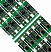
PCB制造
According to relevant definitions, Build up multilayer PCB (BUM) refers to a multilayer printed board with the required number of layers, whICh is formed on an insulating substrate, or on a traditional double-sided board or Multilayer board by coating insulating medium, and then forming wires and connecting holes through electroless copper plating and copper electroplating. As early as the 1970s, BUM technology was reported in the literature, but it was not until the early 1990s that the Japanese branch of IBM developed a new method of coating photosensitive resin on the core board, forming conductive microporous interconnections by photoinduced method, and manufacturing high-density circuit boards by addition method, In 1991, it first published this new technology, calLED Surface Laminar Circuit, SLC (Surface Laminated circuit board). Because this technology created an unprecedented new idea of High Density Interconnect, HDI (High Density Interconnect), Japanese electronic manufacturers began to develop it one after another, which opened the BUM era in the history of PCB development. BUM has adapted to the requirements of electronic products to be lighter, SMAller, thinner and shorter, and can meet the needs of a new generation of electronic packaging technologies (such as BGA, CSP, MCM, FCP, etc.). Therefore, it has developed very rapidly throughout the 1990s and is mainly used in portable electronic products, such as handheld computers, mobile phones, digital CAMeras and MCM packaging substrates. The world BUM microporous plate MARKet was 1.1 billion US dollars in 1998, and nearly 2 billion US dollars in 1999, of which 90% were concentrated in Japan, and the market in 2000 may be close to 3 billion US dollars. DoMEStic experts once wrote a prediction that the world BUM board has entered a development period; At present and in the next few years, the technological transformation and market competition of PCB industry will be carried out around the BUM board as the center and its surrounding industries (materials, equipment, testing, etc.).

1、 Introduction to the manufacturing process of Laminated Multilayer Plate
In contrast to the Japanese who first proposed BUM (Buildup multilayer circuit board), European and American countries later proposed HDI (High Density Interconnect). In fact, these two terms express almost the same conceptual connotation. According to IPC data, the definition of HDI includes the following contents: the non mechanical drilling hole diameter is less than 0.15 mm (6 mil), most of which are blind holes, and the annular ring, pad or land diameter is less than 0.25 mm (6 mil). The holes meeting this condition are called micro holes; PCB with micropores, with contact density of more than 130 points/in2 and wiring density (set channel width as 50mil) of more than 117 inches/in2, is called HDI PCB, and its line width/line spacing (L/S) is 3mil/3mil or less. It can be seen that the most essential feature of multilayer circuit board based on build-up method is high-density interconnection (HDI).
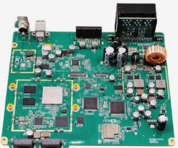
2、 Manufacturing Technology of Multilayer Board
The main difference between BUM and traditional PCB manufacturing process is the hole forming method. The key technologies of BUM mainly include the dielectric materials used in the insulation layer of the built-up layer; Pore forming technology of micro via; Three aspects of hole metallization technology.
Laminated insulating dielectric material
Due to the difference between insulating layer materials and interconnected micropore processing methods, dozens of different BUM manufacturing methods have appeared. However, according to the difference of the laminated insulating medium materials used in different BUM manufacturing processes, the representative and mature processes can be divided into three types: resin coated copper foil (RCC) process, heat cured resin (dry film or liquid) process and photosensitive resin (dry film or liquid) process. Now these three processes are in use. The latter two processes are usually metallized and wired by addition process, which requires high materials and corresponding technologies. The RCC process uses the reduction method to complete the wiring, which does not require a large investment in equipment (the main investment is the laser drill). At the same time, it adapts to the traditional Multilayer PCB manufacturing process, and the finished BUM board has good performance and reliability. Therefore, more and more manufacturers use the RCC process to make BUM boards, and the demand for RCC is increasing. Taking the RCC process as an example, the more layers are built, the worse the flatness of the board surface will be. Due to this limitation, the BUM's build up layer on the core board generally does not exceed 4 layers.
Development Trend of Soft Circuit Board
11-02,2022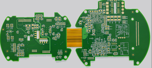


抖音二維碼

Q Q二維碼

微信二維碼
點擊
然后
聯系
然后
聯系
電話熱線
13410863085Q Q

微信

- 郵箱