鑫景福致力于滿足“快速服務,零缺陷,輔助研發”PCBA訂購單需求。


PCB制造
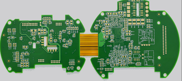
Many hardware engineers or layout engineers are interested in what the inside of a PCB (especially a Multilayer board) looks like when they first contact a PCB. Today, I will take you to understand.

The circuit processing of multilayer PCB is no different from that of single-layer and double-layer PCB. The biggest difference lies in the via process.
The lines are etched, and the vias are drilLED and plated with copper
multilayer circuit boards usually include through hole boards, first order boards, second order boards, and second order perforated boards. Higher order boards, such as third-order boards and interconnection boards at any layer, are seldom used, and the prICe is expensive. I won't discuss it more.
Generally, 8-bit MCU products use 2-layer through-hole boards; The intelligent hardware of 32-bit single chip microcomputer level uses 4-6-layer through-hole boards; Linux and Android level intelligent hardware, using 6-tier through-hole to 8-tier HDI boards; Compact products such as SMArt phones generally use 8-layer 1-level to 10 layer 2-level circuit boards.
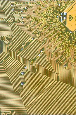
There is only one kind of via, from the first layer to the last layer. No matter the external line or the internal line, the hole is perforated. It is called through-hole plate.
The number of layers has nothing to do with the through-hole board. Usually, the 2-layer through-hole board is used by everyone, while many switches and military circuit boards are made of 20 layers of through-hole boards.
Drill through the circuit board with a drill, and then plate copper in the hole to form a path.
It should be noted here that the inner diameters of through-hole are usually 0.2mm, 0.25mm and 0.3mm, but generally 0.2mm is much more expensive than 0.3mm. Because the drill bit is too thin and easy to break, it is also slow to drill. The cost of more time and drill bit is reflected in the rise in the price of circuit boards.
Laser hole of high density board (HDI board)
The laser can only penetrate glass fiber plates, not metal copper. Therefore, the external surface drilling will not affect other internal lines.
After laser drilling, copper plating is performed to form laser vias.
Ultra expensive arbitrary layer interconnection board, multi-layer laser hole stacking
That is, each layer is a laser hole, and each layer can be connected together. You can route the wire as you want, and punch holes as you want.
Layout engineer thinks it's cool! No longer afraid of painting!
The purchaser wants to cry when he thinks about it. It is more than 10 tiMES more expensive than ordinary through-hole boards!
Therefore, only products like iPhone can be used. For other mobile phone brands, I have never heard of anyone who has used any layer of interconnection board.
The above is the analysis of the internal structure of the PCB.


抖音二維碼

Q Q二維碼

微信二維碼
點擊
然后
聯系
然后
聯系
電話熱線
13410863085Q Q

微信

- 郵箱