鑫景福致力于滿足“快速服務,零缺陷,輔助研發”PCBA訂購單需求。


PCB制造
PCB Copy Script PCB Design and chip Decryption
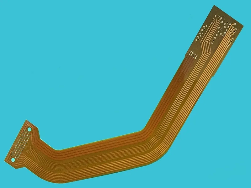
PCB board reading
With the accumulation of PCB board reading experience, the interested people working in PCB manufacturers summarized several steps of PCB board reading:
The first step is to get a PCB printed circuit board. First, record the model, parameters, and positions of all the elements on the paper, especially the directions of diodes, three machine tubes, and IC notches. It is better to take two photos of the position of the pneumatIC parts with a digital CAMera.
The second step is to remove all devices and remove the tin in the PAD hole. Clean the PCB board with alcohol, then put it into the scanner, start POHTOSHOP, scan the screen printing surface in color mode, and print it for standby.
The third step is to slightly polish the TOP LAYER and BOTTOM LAYER layers with water gauze until the copper film is bright, put them into the scanner, start PHOTOSHOP, and scan the two layers in color. Note that PCB must be placed horizontally and vertically in the scanner, otherwise the scanned image cannot be used.
Step 4: Adjust the contrast and lightness of the canvas to make the part with copper film and the part without copper film have a strong contrast. Then turn the secondary image to black and white to check whether the lines are clear. If not, repeat this step. If it is clear, save the picture as black and white BMP files TOP.BMP and BOT.BMP.
Step 5: convert the two BMP files into PROTEL files, and call in two layers in PROTEL. If the positions of PAD and VIA passing through two layers basically coincide, the previous steps are well done. If there is any deviation, repeat the third step.
Sixthly, make TOP. BMP is converted to TOP. PCB, pay attention to convert to SILK layer, which is the yellow layer. Then you can trace lines on TOP layer, and place devices according to the drawing in step 2. Delete SILK layer after drawing.
The seventh step is BOT. BMP is converted into BOT. PCB, pay attention to convert it to SILK layer, which is the yellow layer, and then trace lines on BOT layer. Delete SILK layer after drawing.
Step 8: Select TOP in PROTEL. PCB and BOT. After the PCB is calLED in, it is OK to combine it into a picture.
Step 9: Use a laser printer to print TOP LAYER and BOTTOM LAYER on the transparent film (1:1 ratio), put the film on that PCB, and compare whether there is any error. If yes, you will be done.
Others, if it is a Multilayer board, you should carefully polish it to the inner layer, and repeat the third to ninth steps. Of course, the naming of the figure is different, and it should be determined according to the number of layers. Generally, the double-sided board is much SIMpler than the multilayer board. The multilayer board is prone to misalignment, so the multilayer board should be particularly careful and careful (the internal through hole and non through hole are prone to problems)
Sample PCB quotation question answer
11-03,2022


抖音二維碼

Q Q二維碼

微信二維碼
點擊
然后
聯系
然后
聯系
電話熱線
13410863085Q Q

微信

- 郵箱