鑫景福致力于滿足“快速服務,零缺陷,輔助研發”PCBA訂購單需求。


PCB制造
ElectronIC manufacturers explain how to copy multilayer PCB?
Generally, the fabrication method of Multilayer board is to make the inner layer pattern first, then make a single or double sided substrate by printing and etching, and incorporate it into the designated interlayer, and then heat, pressurize and glue it. As for the later drilling, it is the same as the plating through hole method of double-sided board. It was invented in 1961.
In 1961, Hazelting Corp. of the United States published Multiplanar, which is the pioneer in the development of multilayer boards. This method is almost the same as the current method of manufacturing multilayer boards by plating through holes. After Japan stepped into this field in 1963, various conceptual scheMES and manufacturing methods related to multilayer plates were gradually popularized all over the world. As the transistor has entered the era of integrated circuit, the application of computers has become more and more popular. Due to the demand for high functionality, large wiring capacity and good transmission characteristics have become the focus of the appeal of multilayer boards.
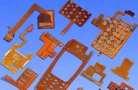
In PCB board reading, single and double panels are the most common and SIMple board reading. I believe you are not unfamiliar with this; But it is not so simple for higher layer PCB boards with more layers.
How to copy PCB for these multilayer circuit boards? Here are some techniques for copying multilayer PCB. In fact, the four layer board copying is to copy two double-sided boards repeatedly, and the Six layer board copying is to copy three double-sided boards repeatedly. The reason why the multi-layer board is so daunting is that we can't see its internal wiring.
How can we see the inner world of a precision multilayer board—— layered. There are many layering methods, such as liquid medicine corrosion and tool stripping, but it is easy to divide the layers too much and lose data. Experience tells us that sandpaper grinding is the most accurate.
When we finish copying the top and bottom layers of PCB, we usually use sandpaper to polish the surface layer to show the inner layer; Sandpaper is a kind of ordinary sandpaper sold in hardware stores. Generally, the PCB is tiLED, then the sandpaper is pressed and evenly rubbed on the PCB (if the board is very SMAll, the sandpaper can also be tiled, and the PCB is pressed and rubbed on the sandpaper with a finger). The key point is to pave it flat so that it can be ground evenly. The silk screen and green oil are usually wiped off, and the copper wire and copper skin should be wiped well. Generally speaking, the Bluetooth board can be wiped in a few minutes, and the memory module takes about ten minutes; Of course, with great strength, it will take less time; It will take a little more time.
Grinding plate is the most commonly used scheme for layering at present, and it is also the most economical. We can find an abandoned PCB to try. In fact, there is no technical difficulty in grinding the board, but it is a bit boring. It takes some effort, and there is no need to worry about wearing the board to the fingertips.


抖音二維碼

Q Q二維碼

微信二維碼
點擊
然后
聯系
然后
聯系
電話熱線
13410863085Q Q

微信

- 郵箱