鑫景福致力于滿足“快速服務,零缺陷,輔助研發”PCBA訂購單需求。


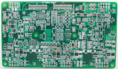
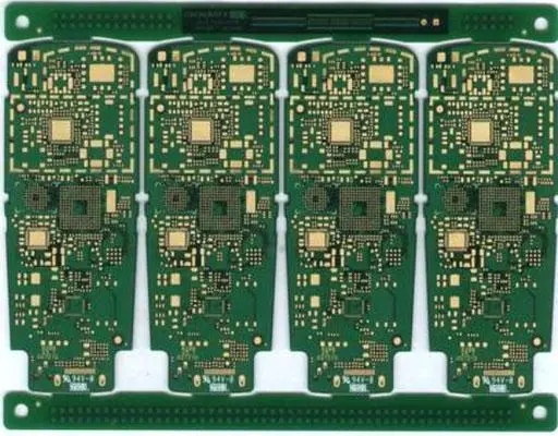
PCB制造
In PCB design, with the rapid increase of frequency, there will be many interferences different from the low frequency PCB design. In actual research, we can conclude that there are mainly four aspects of interference, including power noise, transmission line interference, coupling, and electromagnetIC interference (EMI). By analyzing various interference problems of high-frequency PCB, combined with the practice in work, an effective solution is proposed.

1、 Power noise
In high frequency circuit, the noise of power supply has an obvious effect on high frequency signal. Therefore, the power supply shall be low noise first. Here, clean ground is as important as clean power supply. Why? Obviously, the power supply has a certain impedance, and the impedance is distributed on the whole power supply, so the noise will also be superimposed on the power supply. Then we should reduce the impedance of the power supply as much as possible, so it is better to have a proprietary power layer and ground plane. In high-frequency circuit design, the power supply is designed in the form of layers, which is much better than the bus design in most cases, so that the loop can always follow the path with the least impedance. In addition, the power board must provide a signal loop for all generated and received signals on the PCB, which can minimize the signal loop and thus reduce noise, which is often ignored by low-frequency circuit designers.
There are several methods to eliminate power noise in PCB design:
1. Pay attention to the through-hole on the board: the through-hole makes it necessary to etch an opening on the power layer to make room for the through-hole to pass through. If the opening of the power layer is too large, the signal circuit will be affected, and the signal will be forced to bypass, the circuit area will increase, and the noise will increase. At the same time, if some signal lines are concentrated near the opening and share this loop, the common impedance will cause crosstalk.
2. The connecting line needs enough ground wires: each signal needs its own special signal loop, and the loop area of the signal and loop should be as SMAll as possible, that is, the signal and loop should be parallel.
3. The power supply of analog and digital power supply should be separated: high-frequency devices are generally very sensitive to digital noise, so they should be separated and connected together at the entrance of the power supply. If the signal needs to span both analog and digital parts, a circuit can be placed at the signal crossing point to reduce the area of the loop for the crossing between digital and analog signal circuits.
4. Avoid overlapping of separate power supplies between different layers: otherwise, circuit noise can be easily coupLED through parasitic capacitors.
5. Isolate sensitive components: such as PLL.
6. Placement of power cord: To reduce the signal circuit, the noise is reduced by placing the power cord beside the signal line.
2、 Transmission line
There are only two types of transmission lines in PCB: strip line and microwave line. The biggest problem of transmission lines is reflection, which will cause many problems. For example, the load signal will be the superposition of the original signal and the echo signal, increasing the difficulty of signal analysis; Reflection will cause return loss (return loss), and its impact on signal is as serious as that of additive noise interference:
1. The signal reflected back to the signal source will increase the system noise, making it more difficult for the receiver to distinguish the noise from the signal;
2. Any reflected signal will basically reduce the signal quality and change the shape of the input signal. In general, the solution is mainly impedance matching (for example, the interconnection impedance should match the impedance of the system very well), but sometiMES the impedance calculation is troublesome. You can refer to some transmission line impedance calculation software.
The methods to eliminate transmission line interference in PCB design are as follows:
1. Avoid impedance discontinuity of transmission line. The point of discontinuous impedance is the point of sudden change of transmission line, such as straight corner, through hole, etc., which should be avoided as far as possible. The methods are as follows: avoid the straight corner of the line, and try to walk at a 45 ° angle or arc as much as possible, or at a large angle; Use as few vias as possible, because each vias are impedance discontinuities, and the outer signal shall not pass through the inner layer, and vice versa.
2. Do not use stake lines. Because any pile line is a noise source. If the pile line is short, it can be terminated at the end of the transmission line; If the pile line is long, it will take the main transmission line as the source, which will cause great reflection and complicate the problem. It is recommended not to use it.
3、 Coupling
1. Common impedance coupling: it is a common coupling channel, that is, the interference source and the interfered equipment often share some conductors (such as loop power supply, bus, common grounding, etc.). On this channel, the drop back of the IC causes common mode voltage in the series current loop, which affects the receiver.
2. The field common mode coupling will cause the radiation source to cause common mode voltage on the loop formed by the interfered circuit and the common reference plane. If the magnetic field is dominant, the value of common mode voltage generated in the series grounding circuit is Vcm=- (△ B/△ t) * area (where △ B=variation of magnetic induction intensity). If it is an electromagnetic field, when its electric field value is known, its induced voltage is Vcm=(L * h * F * E)/48, and the formula is applicable to L (m)=150MHz or below. If this limit is exceeded, the calculation of the maximum induced voltage can be SIMplified as: Vcm=2 * h * E.
3. Differential mode field coupling: refers to that direct radiation is induced and received by wire pairs or leads on circuit boards and their loops If it is as close to two wires as possible. This coupling will be greatly reduced, so two wires can be twisted together to reduce interference.
4. Line to line coupling (crosstalk) can make any line equal to the unwanted coupling between parallel circuits, which will greatly damage the performance of the system. It can be classified into capacitive crosstalk and inductive crosstalk. The former is because the parasitic capacitance between lines makes the noise on the noise source coupled to the noise receiving line through current injection; The latter can be thought of as signal coupling between the primary stages of an unwanted parasitic transformer. The size of the inductive crosstalk depends on the proximity of the two loops, the size of the loop area, and the impedance of the affected load.
5. Power line coupling: It refers to that after AC or DC power lines are subject to electromagnetic interference, the power lines transmit these interference to other equipment.
There are several ways to eliminate crosstalk in PCB design:
1. Both crosstalk increases with the increase of load impedance, so signal lines sensitive to interference caused by crosstalk should be properly terminated.
2. The capacitive crosstalk can be effectively reduced by increasing the distance between signal lines as much as possible. Ground plane management, spacing between wiring (such as isolation of active signal lines and ground wires, especially between signal lines with state jump and ground) and reducing lead inductance.
3. Inserting a ground wire between adjacent signal lines can also effectively reduce capacitive crosstalk. This ground wire needs to be connected to the stratum every 1/4 wavelength.
4. For inductive crosstalk, the loop area shall be reduced as much as possible, and if allowed, the loop shall be eliminated. Belonging to Qinji Group, Baineng is a leading electronic industry service platform in China. It provides online components, sensor procurement, PCB customization, BOM distribution, material selection and other complete solutions for the electronic industry supply chain, meeting the comprehensive needs of small and medium-sized customers in the electronic industry in a one-stop manner.
5. Avoid signals sharing loops.
6. Attention to signal integrity: the designer shall realize termination during welding to solve signal integrity. Designers using this approach can focus on the microstrip length of copper foil for shielding in order to obtain good performance of signal integrity. For systems that use dense connectors in communication structures, designers can use a PCB for termination.
4、 Electromagnetic interference
With the increase of speed, EMI will become more and more serious in many aspects (such as electromagnetic interference at the interconnection). High speed devices are particularly sensitive to this, so they will receive high-speed false signals, while low-speed devices will ignore such false signals.
There are several methods to eliminate electromagnetic interference in PCB design:
1. Reduce loops: Each loop is equivalent to an antenna, so we need to minimize the number of loops, the area of loops, and the antenna effect of the loop. Ensure that the signal has only one loop path at any two points, avoid artificial loops, and try to use the power layer.
2. Filtering: filtering can be adopted on both power lines and signal lines to reduce EMI. There are three methods: decoupling capacitor, EMI filter and magnetIC components.
3. Shield and minimize the speed of high-frequency devices.
4. Increase the dielectric constant of the PCB board to prevent the transmission line near the board and other high-frequency parts from radiating outward; Increasing the thickness of PCB board and minimizing the thickness of microstrip line can prevent the overflow of electromagnetic lines and also prevent radiation.
So far, we can conclude that in the design of high-frequency PCB, we should follow the following principles:
1. Unification and stability of power supply and ground.
2. Careful cabling and proper termination can eliminate reflections.
3. Careful cabling and proper termination can reduce capacitive and inductive crosstalk.
4. Noise suppression is required to meet EMC requirements.


抖音二維碼

Q Q二維碼

微信二維碼
點擊
然后
聯系
然后
聯系
電話熱線
13410863085Q Q

微信

- 郵箱