鑫景福致力于滿足“快速服務(wù),零缺陷,輔助研發(fā)”PCBA訂購單需求。


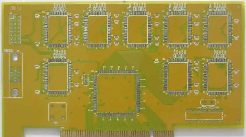
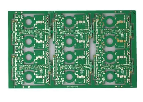
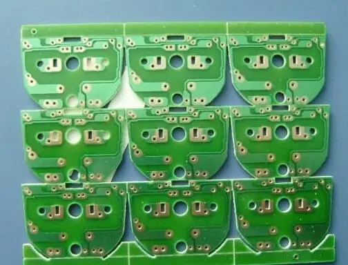
PCB制造
PCB copper foil thICkness, line width and maximum load current
Thickness of copper foil – ounces (ounce, oz)
The thickness of copper foil commonly used in the industry is "oz", but "oz" is clearly the weight, how can it become the thickness again? This is because in the terminology of copper skin, the "ounce" has been converted into a unit of thickness. The more you listen to it, the more confused you become? This is because the specification of the copper sheet is defined by the number of ounces per square foot (ft2), so we often say that 1oz is the weight of 1oz per square foot (ft2). The thicker the copper sheet, the heavier it will be. Because the weight of the copper sheet is proportional to the thickness, the ounces of the copper sheet can be equivalent to the thickness, and can be converted into millimeters (mm) or milliinches (mils). In fact, this is a little SIMilar to the calculation in pounds when we calculate the paper. If you are interested, check it yourself!
Here are some commonly used dimensions, which are converted into mils and mm for your reference:
0.5 oz=0.0007 inch=0.7 mils=0.018 mm
1.0 oz=0.0014 inch=1.4 mils=0.035 mm
2.0 oz=0.0034 inch=2.8 mils=0.070 mm
Now we also try to calculate why the 1oz copper foil is about 1.4 mils:
The specific gravity of copper is 8.9 (gm/cm3),
Unit conversion: 1 (ft2)=93055 (mm2), 1 (mil)=2.54 (um), 1 (oz)=28.34 (gm)
1oz volume=28.34 (gm)/8.9 (gm/cm3)=3.1842 (cm3)=3184.2 (mm3)
1oz thickness=3184.2 (mm3)/93055 (mm2)=0.03422 (mm)=1.35 (mils)
Note: The density of copper foil varies with the use of different copper, so there may be some SMAll errors in the calculation.
Relationship between PCB copper foil sectional area and maximum load current and temperature rise
According to Section 6.2 (Conductive Material Requirements) of IPC-2221, the maximum current carrying capacity of the circuit board can be divided into two types: inner layer circuit and outer layer circuit, and the maximum current carrying capacity of the inner layer circuit is set to be only half of that of the outer layer circuit. Chart 6-4 of IPC-2221 is excerpted here to illustrate the relationship between the copper foil sectional area, temperature rise and the maximum current carrying capacity of external conductors and internal conductors.
In addition, someone cleverly summarized a formula for the relationship between the current carrying capacity of the above PCB lines, which can be roughly used to replace the results obtained by looking up the table:
I = K△T0.44A0.75
K: As a correction factor, it is generally 0.024 for the inner layer of copper clad wire and 0.048 for the outer layer.
△ T: refers to the maximum temperature difference, indicating that the temperature of copper foil after being energized is higher than the ambient temperature, and the unit is Celsius (° C)
A: Is the sectional area of copper clad line, in square milliinch (mil2)
1: Is the current carrying capacity (Amp)
1(mil) = 25.4(um)
In the section with many pads (pads), the current carrying capacity of the line with tin after passing through the furnace will be greatly increased. I believe that many people have seen a section of the line between the pad and the pad burned in some high current plates. The reason is simple, because there is more solder on the pad, that is, the area of the line that can withstand the current is increased, However, the circuit between the welding pad and the welding pad has not changed at all. Therefore, when the power supply is just started or when the circuit executes command conversion, it is very likely to cause excessive current Surge. At this time, it is easy to burn off the circuit with weak current carrying capacity between the welding pad and the welding pad.
The solution is to increase the width of the conductor. If the board cannot allow the conductor to increase the width, you can also consider turning on the solder mask on the lines that are easy to burn, and using the SMT process to add solder paste. After reflow, the thickness of the conductor can be increased, which increases the current carrying capacity.


抖音二維碼

Q Q二維碼

微信二維碼
點擊
然后
聯(lián)系
然后
聯(lián)系
電話熱線
13410863085Q Q

微信

- 郵箱