鑫景福致力于滿足“快速服務,零缺陷,輔助研發”PCBA訂購單需求。


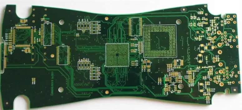
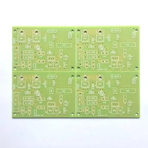
PCB制造
During PCB design, if possible risks can be predICted in advance and avoided in advance, the success rate will be greatly improved. Many companies will have an indicator of the success rate of PCB design when evaluating projects.
The key to improve the success rate of the first board is the signal integrity design. In the current electronic system design, there are many product solutions that chip manufacturers have prepared, including what chips to use and how to build peripheral circuits. Hardware engineers rarely need to consider the principle of the circuit board, and only need to make the PCB themselves.
However, it is in the process of PCB design that many enterprises encounter difficulties, either the PCB design is unstable or does not work. For large enterprises, many chip manufacturers will provide technical support to guide PCB design. However, it is difficult for some SMAll and medium-sized enterprises to obtain such support. Therefore, we must find a way to complete it by ourselves, so there are many problems, which may require several versions, and debugging takes a long time. In fact, if we understand the design method of the system, these can be completely avoided. Next, let's talk about three techniques to reduce PCB design risk.
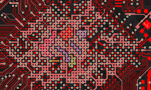
First, in the system planning stage, it is better to consider the signal integrity. The whole system is built in this way. Can signals be received correctly when they are transferred from one PCB to another? This needs to be evaluated in the early stage, but it is not difficult to evaluate this problem. A little knowLEDge of signal integrity and a little SIMple software operation can do it.
2. During PCB design, use simulation software to evaluate specific PCB routing and observe whether the signal quality can meet the requirements. The simulation process itself is very simple. The key is to understand the principle knowledge of signal integrity and use it for guidance.
Third, risk control must be carried out during PCB manufacturing. There are many problems. At present, there is no way to solve the simulation PCB software, which must be manually controlled by the designer. The key to this step is to understand where there are risks and how to avoid them. What is needed is signal integrity knowledge.
If we can grasp these three points in the PCB design process, the PCB design risk will be greatly reduced, the probability of error will be much smaller after the printing, and debugging will be relatively easy.


抖音二維碼

Q Q二維碼

微信二維碼
點擊
然后
聯系
然后
聯系
電話熱線
13410863085Q Q

微信

- 郵箱