鑫景福致力于滿足“快速服務(wù),零缺陷,輔助研發(fā)”P(pán)CBA訂購(gòu)單需求。


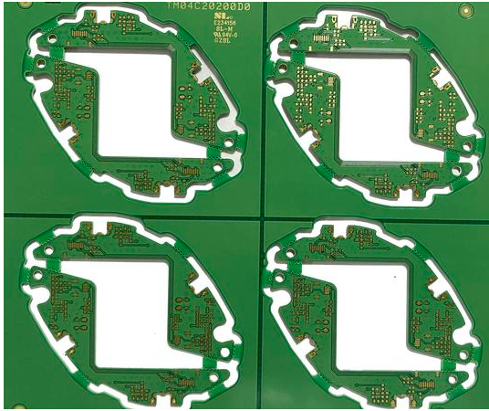
PCB制造
Signal Integrity (SI for short) of high-speed PCB board sub design generation processing signal integrity
Definition: The quality of the signal on the signal line is the ability of the signal to respond with correct timing and voltage in the circuit.
High switching speed of integrated circuit chips (ICs) or logic devices, incorrect layout of terminal components or wrong wiring of high-speed signals will cause signal integrity problems such as reflection, crosstalk, overshoot, undershoot, ringing, etc., which may cause the system to output incorrect data, and the circuit will not work normally or even completely.
Signal Integrity and design of PCB
In PCB design, PCB designers need to integrate the layout and wiring of components and what SI problem solving methods should be used in each case to better solve the signal integrity problem of PCB. In some cases, the selection of IC can determine the number and severity of SI problems Switching time or edge rate refers to the rate of IC state transition. The faster the IC edge rate is, the higher the possibility of SI problems. It is important to correctly terminate components. A common way to reduce signal integrity problems in PCB design is to add terminating components on the transmission line. In the termination process, it is necessary to balance the requirements of the number of components, signal switching speed and circuit power consumption For example, adding termination components means that PCB designers have less space for wiring, and it will be more difficult to add termination components in the later stage of layout processing, because corresponding space must be reserved for new components and wiring. Therefore, it should be clear whether termination components need to be placed at the initial stage of PCB layout
1. General criteria for signal integrity design:
How to define the number of PCB layers?
How many layers are included? How to arrange the content of each layer in the most reasonable way? For example, there should be several layers of signal layer, power layer and stratum, and how the signal layer and stratum are alternately arranged
How to design multiple power block systems?
For example, 3.3V, 2.5V, 3V, 1.8V, 5V, 12V, etc. The reasonable division of the power layer and the common ground problem are very important factors for PCB stability
How to configure decoupling capacitor?
Using decoupling capacitor to eliminate noise is a common method, but how to determine its capacitance? Where is the capacitor placed? What type of capacitor is used?
How to eliminate ground bounce noise?
How does ground missile noise affect and interfere with useful signals?
How to eliminate the Return Path noise? In many cases, unreasonable loop design is the key to the failure of the circuit, and loop design is often the most helpless work of engineers.
How to reasonably design the current distribution?
In particular, it is very difficult to design the current distribution in the electrical/stratum, and if the total current is distributed unevenly in the PCB, it will directly and significantly affect the unstable operation of the PCB.
In addition, there are some common problems related to signal distortion, such as overshoot, undershoot, ringing, transmission line delay, impedance matching, crosstalk, burr, etc., but these problems are inseparable from the above problems, and they are causal
High Speed PCB design
2. PCB design criteria to ensure signal integrity
The earlier the signal integrity (SI) problem is solved, the more efficient the design will be, thus avoiding adding termination components after the circuit board design is completed With the increase of IC output switching speed, almost all designs encounter signal integrity problems regardless of signal cycle Even though there is no SI problem in the past, with the increase of circuit operating frequency, there will be signal integrity problems SI and EMC experts need to conduct SIMulation and calculation before PCB wiring. Then, PCB design can follow a series of very strict design rules. In case of doubt, termination components can be added to obtain as much SI safety margin as possible Power supply integrity (PI) is closely related to signal integrity (SI). Power supply integrity directly affects the signal integrity of the final PCB. In many cases, the main reason that affects signal distortion is the power supply system At present, EMC design mainly adopts the method of design rule checking. It is important for enterprises to gradually establish and improve design specifications that are suitable for products in specific areas of the enterprise to form a complete set of EMC design rule sets. These are very popular in large foreign companies, such as Samsung and SONY. These rules are checked by people or EDA software
3. Electrostatic discharge (ESD) design of PCB
Many product design engineers usually start to consider the problem of anti-static discharge (ESD) when products enter the production process. If the electronic equipment cannot pass the anti-static discharge test, the final solution usually requires expensive components, manual assembly in the manufacturing process, or even redesign. Therefore, the product schedule is bound to be affected. Even experienced PCB design engineers may not know which parts of the design are conducive to anti-static discharge (ESD). Most Electronic devices spend 99% of their life in an environment full of ESD, which may not come from the human body, furniture, or even the equipment itself. It is rare for electronic equipment to be completely damaged by ESD. However, ESD interference is very common, which will lead to equipment lock, reset, data loss and unreliability. The result may be that electronic equipment often breaks down in cold and dry winter, but it shows normal during maintenance, which will inevitably affect users' confidence in electronic equipment and its manufacturers.
4. ESD generation mechanism
When a conductor that allows electricity is close to another conductor, a strong electric field will be established between the two conductors, resulting in breakdown caused by the electric field. When the voltage between two conductors exceeds the breakdown voltage of the air and insulating medium between them, ESD arc will be generated. In 0.7ns to 10ns, the ESD arc current will reach tens of amperes or even more than 100A. The ESD arc will generate a strong magnetic field with a frequency range of 1MHz~500MHz, and inductively couple to each adjacent wiring loop, generating a current of more than 15A and a high voltage of more than 4KV within 10cm from the ESD arc. The ESD arc will be maintained until two conductors are short circuited or the current is too low to maintain the arc.
5. ESD resistant PCB layout and PCB wiring design
Multi layer PCB board structure shall be used as far as possible, and special power supply and ground plane shall be arranged in the inner layer of PCB board. Bypass and capacitor stripping are adopted. As far as possible, each signal layer should be close to a power supply layer or ground wire layer. For high-density PCBs with components on the top and bottom surfaces, short connecting lines, and many filling grounds, inner layer wiring can be considered.
Ensure that the Layout of components between each functional circuit and each functional circuit is as compact as possible. For circuits or sensitive components susceptible to ESD, they should be placed near the center of the PCB, so that other circuits can provide them with a certain shielding effect. In the area that can be directly hit by ESD, a ground wire shall be laid near each signal line.
At the I/O interface of the equipment easily accessible to ESD and at the position where people often need to touch or operate, such as reset key, communication port, on/off key, function key, etc. Generally, transient protectors, series resistors or magnetic beads are placed at the receiving end.
Make sure the signal line is as short as possible. When the length of the signal line is greater than 12inch (30cm), a ground wire must be laid in parallel.
Make sure that the loop area between the signal line and the corresponding loop is as SMAll as possible. For long signals, change the position of the signal line and the ground wire every few centimeters or inches to reduce the loop area.
Ensure that the loop area between the power supply and the ground is as small as possible, and place a high-frequency capacitor near each power pin of the integrated circuit chip (IC).
If possible, fill unused areas with land, and connect the filling ground of all layers every<2inch (5cm).
When the length of the opening on the power supply or ground plane exceeds 8mm, use narrow wires to connect the two sides of the opening.
The reset line, interrupt signal line, or edge trigger signal line cannot be arranged near the edge of the PCB.


抖音二維碼

Q Q二維碼

微信二維碼
點(diǎn)擊
然后
聯(lián)系
然后
聯(lián)系
電話熱線
13410863085Q Q

微信

- 郵箱