鑫景福致力于滿足“快速服務,零缺陷,輔助研發”PCBA訂購單需求。


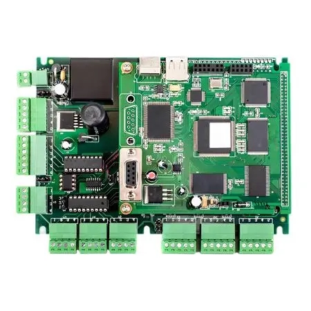
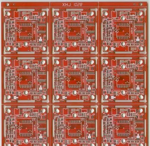
PCB制造
Pcb factory: quality control of solder paste printing process
In the reflow soldering of surface mount assembly, solder paste is used for the connection between the pins or terminals of surface mount components and pads. There are many variables, such as solder paste, screen printing machine, solder paste applICation method and printing process. In the process of printing solder paste, the base plate is placed on the workbench, clamped and positioned mechanically or vacuum, and aligned with locating pins or vision. Or screen or stencil for solder paste printing. This paper will focus on several key solder paste printing issues, such as template design and printing process. Printing process and equipment
In the reflow soldering of surface mount assembly, solder paste is used for the connection between the pins or terminals of surface mount components and pads. There are many variables, such as solder paste, screen printing machine, solder paste application method and printing process. In the process of printing solder paste, the base plate is placed on the workbench, clamped and positioned mechanically or vacuum, and aligned with locating pins or vision. Or screen or stencil for solder paste printing. This paper will focus on several key solder paste printing issues, such as template design and printing process.
Printing process and equipment
In the solder paste printing process, the printing machine is the key to achieve the desired printing quality.
In the manual or sEMI-automatic printing machine, the solder paste is manually placed on the template/screen, and the squeegee is at the other end of the template. In the automatic printing machine, solder paste is automatically distributed. During printing, the printing scraper presses down on the template to make the bottom surface of the template contact the top surface of the circuit board. When the scraper passes the entire length of the corroded graphic area, the solder paste is printed on the pad through the opening on the template/screen.
After the solder paste has been deposited, the screen will snap off immediately after the scraper and return to the original place. This interval or separation distance is determined by the equipment design, about 0.020 "~0.040". The separation distance and scraper pressure are two important variables related to equipment to achieve good printing quality. If not, this process is calLED on contact printing. When using all metal templates and scrapers, use contact printing. Off contact printing is used for flexible wire MESh.
Squeegee type
The abrasion, pressure and hardness of the scraper determine the printing quality, which should be carefully monitored. For acceptable printing quality, the scraper edge should be sharp and straight. Low scraper pressure will cause missing and rough edges, while high scraper pressure or very soft scraper will cause smudged printing, and may even damage the scraper, template or screen. Excessive pressure also tends to dig out solder paste from wide openings, resulting in insufficient solder fillets.
There are two common types of scrapers: rubber or polyurethane scrapers and metal scrapers. When using a rubber scraper, use a 70-90 durometer hardness scraper. When the pressure is too high, the solder paste that seeps into the bottom of the template may cause a tin bridge, which requires frequent bottom wiping. In order to prevent the penetration of the bottom, the pad opening must provide a sealing function during printing. This depends on the roughness of the formwork opening wall.
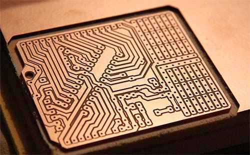
Stencil type
Important printing quality variables include the precision and finish of the template hole wall. It is important to save the appropriate aspect ratio of the template width and thickness. The recommended aspect ratio is 1.5. This is important to prevent the template from blocking. Generally, if the aspect ratio is less than 1.5, the solder paste will remain in the opening. In addition to aspect ratio, as recommended in IPC-7525 Template Design Guide, there is also an area ratio greater than 0.66 (pad area divided by hole wall area). IPC-7525 can be a good starting point for template design.
The technological process of making the hole controls the smoothness and accuracy of the hole wall. There are three common processes for making templates: chemical etching, laser cutting and additive process.
Chemically etched formwork
The metal template and flexible metal template are etched by chemical grinding from both sides using two positive patterns. In this process, etching is carried out not only in the desired vertical direction, but also in the horizontal direction. This is called undercutting - the hole is larger than expected, resulting in additional solder deposition. Because 50/50 is etched from both sides, the result is a nearly straight hole wall with a slight hourglass shaped narrowing in the middle.
Because the hole wall of the electroetching template may not be smooth, electropolishing, a micro etching process, is a method to achieve smooth hole wall. Another method to achieve a smoother hole wall is nickel plating. The polished or smooth surface is good for the release of solder paste, but it may cause the solder paste to cross the template surface without rolling in front of the scraper. This problem can be avoided by selectively polishing the hole wall instead of the entire template surface. Nickel plating further improves smoothness and printability. However, it reduces the opening and requires graphic adjustment
Laser cut template
Laser cutting is another subtractive process, but it has no undercut problem. The template is directly made from Gerber data, so the opening accuracy is improved. The data can be adjusted as needed to change the size. Better process control will also improve the opening accuracy. Another advantage of the laser cutting template is that the hole wall can be tapered. The chemically etched template can also be tapered. If it is etched from only one side, the opening size may be too large. The opening of the plate surface is slightly larger than the conical opening of the scraping plate surface (0.001 "~0.002", generating an angle of about 2 °), which makes it easier to release the solder paste.
Laser cutting can produce a hole width as SMAll as 0.004 "with an accuracy of 0.0005", so it is very suitable for ultra fine pitch component printing. The template cut by laser will also produce rough edges, because the metal vaporized during cutting will become metal slag. This may cause the solder paste to jam. A smoother hole wall can be produced by micro etching. If the laser cut template has not been chemically etched on the area that needs to be thinner in advance, it cannot be made into a stepped multi-stage template. The laser cuts each hole one by one, so the template cost depends on the number of holes to be cut.
Electroformed template
The third process for making templates is an addition process, most commonly called electroforming. In this process, nickel is deposited on the copper cathode core to form an opening. A photosensitive dry film is laminated on a copper foil (about 0.25 "thick). The film is polymerized by ultraviolet light through a mask with a template pattern. After development, a cathode pattern is generated on the copper centroid, and only the template opening is kept with a photoresist Override. Then a template is formed around the photoresist by nickel plating. After the desired template thickness is reached, remove the photoresist from the opening. The electroformed nickel foil is separated from the copper core by bending - a key process step. Now the foil is ready for framing and other steps for making the template.
Electroforming step formwork can be done, but the cost is increased. Due to the precision tolerance, the electroformed formwork provides a good sealing effect and reduces the solder paste leakage on the bottom of the formwork. This means that the frequency of wiping the bottom of the template is significantly reduced, reducing the potential tin bridge.
PCB manufacturers and PCB designers will explain the quality control of solder paste printing process.


抖音二維碼

Q Q二維碼

微信二維碼
點擊
然后
聯系
然后
聯系
電話熱線
13410863085Q Q

微信

- 郵箱