鑫景福致力于滿足“快速服務,零缺陷,輔助研發”PCBA訂購單需求。


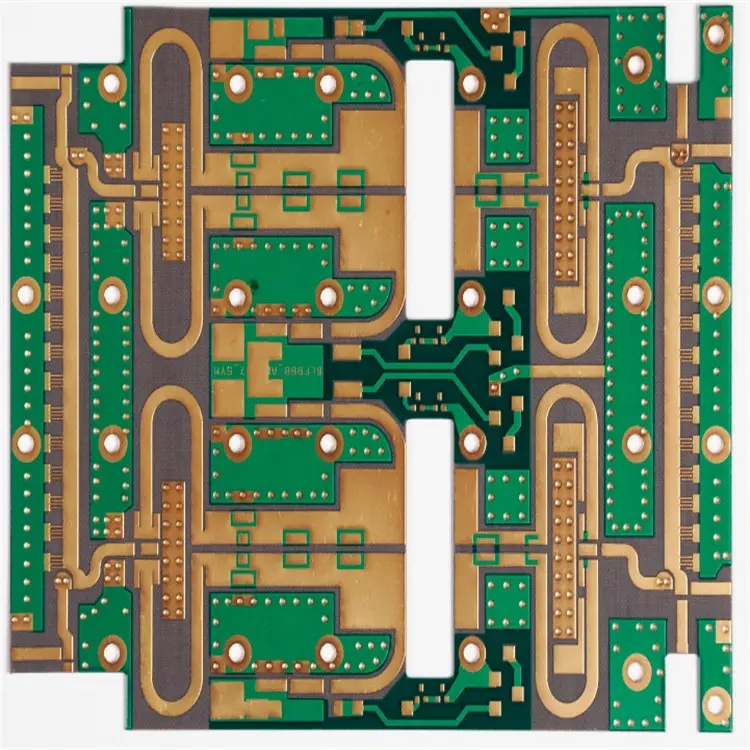
PCB制造
Use liquid gasifICation latent heat to check the tin and solder joints on the circuit board?
The so-calLED latent heat of liquid gasification refers to the total amount of heat that a specific liquid with high gasification heat needs to absorb during the gasification process. Take water as an example. When it is heated to 100 ° C, the temperature will stop rising. However, 540kcal/g of heat energy is needed to turn water into steam. In the same way, when the operator selects a certain high latent heat organic solvent, he can use the liquid to reach the volatile state to accumulate the latent heat. By using the latent heat transfer generated by the phase change of this material, the solder can be melted to achieve the purpose of welding. This operation method is vapor condensation tin method (VCS
The so-called latent heat of liquid gasification refers to the total amount of heat that a specific liquid with high gasification heat needs to absorb during the gasification process. Take water as an example. When it is heated to 100 ° C, the temperature will stop rising. However, 540kcal/g of heat energy is needed to turn water into steam. In the same way, when the operator selects a certain high latent heat organic solvent, he can use the liquid to reach the volatile state to accumulate the latent heat.
The latent heat transfer generated by the phase change of this material can be used to melt the solder to achieve the purpose of welding, This operation method is vapor condensation Soldering (VCS - Vapor [Condensation Soldering] ing) or vapor phase Soldering (VPS - VaporPhase Soldering). The difference between this method and the previous method is that it uses the latent heat of liquid phase change to melt solder, which is a circuit board welding method developed in the United States in 1973.
PCB with tin coating
The use of the latent heat of gasification and the heat released when the gas condenses into a liquid can bring stable and sufficient heat to the circuit board welding parts. As long as the liquid medium is appropriate, even if the heat required by the parts is quite large, the operating temperature should be kept constant. When the tinned parts are fed into the saturated vapor filled with solvent, the parts touching the vapor will absorb heat and generate gas condensation to release latent heat. In order to prevent saturated steam from diffusing outwards, steam condensation coil will be installed above such devices to cool and recover solvent. The advantages of this circuit board welding method are as follows:
(1) The tin loading temperature can be controlled correctly by using the physical property of the latent heat of gasification.
(2) It is not affected by the shape and heat capacity of tinned parts, and can be heated uniformly.
(3) It can generate tin space shielding on the circuit board to reduce solder surface activity, and the parts will not be oxidized.
(4) The medium has fast heat transfer and large latent heat, which can overcome the welding problem of dead angle and large parts.
The latent heat is used as the heat source for melting tin, and the solvent used is very important. The general conditions for solvent use are based on the principle that the latent heat can meet the tin coating temperature, non-toxic, and high thermal stability. The solvent that can meet this condition is a more appropriate choice. Typical equipment design includes vertical design made of batch circuit boards and horizontal conveyor belt design. Typical conveying equipment structure,
How to effectively check solder joints of circuit boards?
In general, solder joint inspection of circuit boards can be performed by visual inspection, automatic optical inspection (AOI), X-ray inspection, infrared laser inspection, ultrasonic microscopy, etc. Visual inspection can find solder skips, bridging, wettability, part alignment, solder beads, etc., but cannot detect internal structural defects. The accuracy rate of visual inspection is not stable, which generally falls below 75-85%. At the same time, manual inspection is limited by the speed limit, and the number of I/Os that can be checked per second is not high. At the same time, the results of visual inspection are highly related to the inspector, which is also the biggest source of instability of this kind of practice. The following figure shows the situation of manual inspection after the general line.
In general, solder joint inspection of circuit boards can be performed by visual inspection, automatic optical inspection (AOI), X-ray inspection, infrared laser inspection, ultrasonic microscopy, etc. Visual inspection can find solder skips, bridging, wettability, part alignment, solder beads, etc., but cannot detect internal structural defects. The accuracy rate of visual inspection is not stable, which generally falls below 75-85%. At the same time, manual inspection is limited by the speed limit, and the number of I/Os that can be checked per second is not high. At the same time, the results of visual inspection are highly related to the inspector, which is also the biggest source of instability of this kind of practice. The following figure shows the situation of manual inspection after the general line.
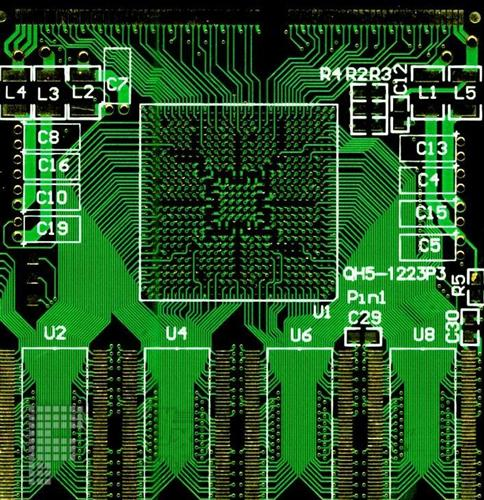
Perform a visual inspection of the circuit board
If the Circuit board manufacturer can set some product relative quality standards, it can perform automatic optical inspection on the appearance of the solder joint, which can SIMplify the quality inspection of the solder joint of the circuit board and improve the stability of the overall inspection. At present, most of the automatic inspection equipment have established a quality database. As long as the inspection level is added, appearance inspection can be carried out quickly. The X-ray system is suitable for checking virtual points, open circuits, hidden solder beads, hidden short circuits, skewed circuit board solder joints, etc. The commonly used systems are perspective X-ray system and section X-ray system. The following figure shows typical SMT optical inspection image and BGA part solder joint bubble image.
The infrared laser inspection system uses controllable pulses to heat the solder joint surface in a SMAll amount, and the generated temperature rise and fall curve becoMES the detection signal of the solder joint. Compare the position of each solder joint on the circuit board with the qualified signal, and determine whether it is good or bad according to the given standard in advance. Ultrasound microscopy can produce very high image recognition rate. The commonly used ultrasonic frequency range is 10-500MHz or higher.


抖音二維碼

Q Q二維碼

微信二維碼
點擊
然后
聯系
然后
聯系
電話熱線
13410863085Q Q

微信

- 郵箱