鑫景福致力于滿足“快速服務(wù),零缺陷,輔助研發(fā)”PCBA訂購單需求。


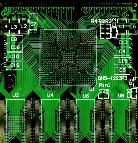
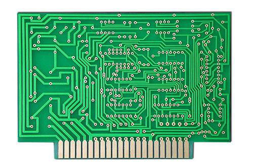
PCB制造

An important way to reduce EMI is to design PCB ground plane. The step is to make the grounding area within the total area of PCB circuit board as large as possible, so as to reduce emission, crosstalk and noise. Special care must be taken when connecting each component to the grounding point or ground plane. If this is not done, the neutralization effect of reliable ground plane cannot be fully utilized.
A partICularly complex one has several stable voltages. Ideally, each reference voltage has its own corresponding ground plane. However, if there are too many ground planes, the manufacturing cost of PCB will be increased and the price will be too high. The compromise is to use grounding layers at three to five different locations, each of which can contain multiple grounding parts. This not only controls the manufacturing cost of the circuit board, but also reduces EMI and EMC.
If you want EMC, low impedance grounding system is very important. In a multilayer PCB, there is a reliable ground plane, not a copper balancing block or a scattered ground plane, because it has low impedance, can provide a current path, and is a reverse signal source.
The length of time the signal returns to the ground is also important. The time for signals to return to and from the signal source must be equal, otherwise, a phenomenon SIMilar to an antenna will occur, making the radiated energy a part of EMI. Similarly, the routing of the current to/from the signal source should be as short as possible. If the length of the source path and the return path is not equal, the grounding rebound will occur, which will also cause EMI.

PCB grounding
If the time of signals entering and leaving the signal source is not synchronized, a phenomenon similar to the antenna will occur, which will radiate energy and cause EMI
Tip 2: Differentiate EMI
Due to different EMI, a good EMC design rule is to separate analog circuits from digital circuits. Analog circuits with high amperage or current should be far away from high-speed wiring or switch signals. If possible, they should be protected with an earth signal. On, the wiring of analog wiring should be on one ground plane, while the switch wiring or high-speed wiring should be on another ground plane. Therefore, signals with different characteristics are separated.
SometiMES a low-pass filter can be used to eliminate the high-frequency noise coupLED with the surrounding wiring. The filter can suppress noise and return stable current. It is important to separate the ground plane of analog signal and digital signal. Because analog circuit and digital circuit have their own unique characteristics, it is very important to separate them. Digital signals shall have digital grounding, and analog signals shall terminate at analog grounding.
In digital circuit design, experienced PCB layout and design engineers will pay special attention to high-speed signals and clocks. At high speeds, signals and clocks should be as short as possible and adjacent to the ground plane, because, as previously mentioned, the ground plane can keep crosstalk, noise and radiation in a controllable range.
Digital signals should also be away from the power plane. If the distance is very close, noise or induction will be generated, thus weakening the signal.
Tip 3: Crosstalk routing is important
Wiring is particularly important to ensure the normal flow of current. If the current comes from an oscillator or other similar equipment, it is particularly important to separate the current from the ground plane or not to allow the current to run in parallel with another line. Two parallel high-speed signals will generate EMC and EMI, especially crosstalk. The resistance path must be kept short and the return current path as short as possible. The length of the return path route should be the same as the length of the send route.
For EMI, one is called "violation route", and the other is "victim route". Inductive and capacitive coupling will affect the "victim" routing due to the existence of electromagnetic field, thus generating forward and reverse currents on the "victim" routing. In this way, ripple will be generated in a stable environment where the transmission length and reception length of the signal are almost equal.
In an environment with good balance and stable routing, the induced currents should cancel each other to eliminate crosstalk. However, we are in an imperfect world, and this will not happen. Therefore, our goal is to keep the crosstalk of all routing lines at a level. If the width between parallel routes is twice of the route width, the crosstalk effect can be reduced. For example, if the route width is 5 mils, the distance between two parallel routes should be 10 mils or more.
With the continuous emergence of new materials and components, PCB designers must continue to deal with electromagnetic compatibility and interference problems.
Tip 4: Decoupling capacitors
Decoupling capacitors can reduce the adverse effects of crosstalk. They should be located between the power supply pin and the grounding pin of the device, which can ensure low AC impedance and reduce noise and crosstalk. In order to achieve low impedance over a wide frequency range, multiple decoupling capacitors should be used.
An important principle for placing decoupling capacitors is that capacitors with capacitance values should be as close to the equipment as possible to reduce the inductance impact on the wiring. This specific capacitor shall be as close to the power supply pin or power wiring of the equipment as possible, and the bonding pad of the capacitor shall be directly connected to the via or ground plane. If the wiring is long, use multiple vias to make the grounding impedance.
Tip 5: Avoid 90 ° angles
To reduce EMI, avoid wiring, vias and other components from forming a 90 ° angle, because the right angle will generate radiation. At this angle, the capacitance will increase, and the characteristic impedance will also change, resulting in reflection, and then EMI. To avoid a 90 ° angle, the wiring should be routed to the corner at least at two 45 ° angles.
Tip 6: Use vias with caution
In almost all cases, vias must be used to provide conductive connections between different layers. PCB layout engineers need to be very careful because vias can generate inductance and capacitance. In some cases, they also produce reflections because the characteristic impedance changes when vias are made in the routing.
It is also important to remember that the vias will increase the routing length and need to be matched. In case of differential wiring, vias shall be avoided as far as possible. If it cannot be avoided, vias should be used in both routes to compensate for delays in the signal and return paths.
Tip 7: Cable/Physical Shielding
The cable carrying digital circuit and analog current will generate parasitic capacitance and inductance, causing many EMC related problems. If twisted pair cables are used, the coupling level will be kept low and the magnetic field generated will be eliminated. For high-frequency signals, shielded cables must be used, with the front and back grounded to eliminate EMI interference.
Physical shielding is to wrap the whole or part of the system with metal packaging to prevent EMI from entering PCB circuit. This shield acts like a closed, grounded conductive container, reducing the size of the antenna loop and absorbing EMI.


抖音二維碼

Q Q二維碼

微信二維碼
點(diǎn)擊
然后
聯(lián)系
然后
聯(lián)系
電話熱線
13410863085Q Q

微信

- 郵箱