鑫景福致力于滿足“快速服務,零缺陷,輔助研發”PCBA訂購單需求。


PCB制造
manufacturing process of single-sided PCB and double-sided PCB
Single sided PCB refers to the circuit board with conductive pattern on only one side, whICh is generally made of phenolic resin paper based copper clad plate. The typical manufacturing process is as follows.
Single sided copper clad laminate → blanking (brushing and drying) → drilling or punching → screen printing of anti etching patterns or use of dry film → curing, inspection and repair → etching of copper → removal of anti etching printing materials and drying → brushing and drying → screen printing solder resistance patterns (commonly used green oil), UV curing → screen printing character MARKing patterns, UV curing → punching and shape processing → electrical opening and short circuit test → brushing Drying → precoating anti oxidant flux (drying) or tin spraying hot air leveling → packaging inspection → finished products leaving the factory.
Manufacturing Process of Double sided PCB
Double sided PCB refers to the circuit board with conductive patterns on both sides. It is usually made of epoxy glass cloth copper clad foil, and is mainly used in communication electronic equipment, advanced instruments and meters, electronic computers and other equipment with high performance requirements. The typical process for manufacturing double-sided plated hole printed boards is the bare copper solder mask coating process (SMOBC). The process is as follows.
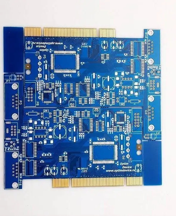
Double sided PCB
Double sided copper clad plate → blanking → lamination → CNC drilling through hole → inspection, deburring and brushing → chEMIcal plating (metallization of through hole) → (plating thin copper on the whole plate) → inspection and brushing → screen printing negative circuit graphics, curing (dry film or wet film, exposure and development) → inspection Trimming → circuit pattern electroplating → electrotinning (corrosion resistant nickel/gold) → printing material (photosensitive film) → etching copper → (tin removal) → cleaning and brushing → printing solder resistance figures with heat curing green oil screen (pasting photosensitive dry film or wet film, exposure, development, heat curing, commonly used photosensitive heat curing green oil) → cleaning, drying → screen printing characters and figures, curing → (tin spraying or organic solder mask) → shape processing → cleaning Drying → electrical on/off detection → packaging inspection → finished products leaving the factory.
PCB manufacturing, PCB design and PCBA processing manufacturers will explain the manufacturing process of single-sided PCB and double-sided PCB


抖音二維碼

Q Q二維碼

微信二維碼
點擊
然后
聯系
然后
聯系
電話熱線
13410863085Q Q

微信

- 郵箱