鑫景福致力于滿足“快速服務,零缺陷,輔助研發(fā)”PCBA訂購單需求。


PCB制造
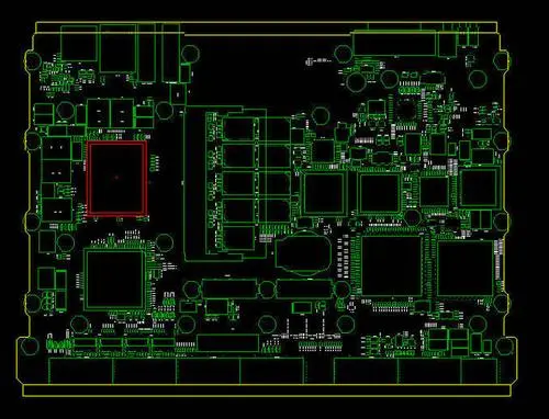
Pcb board (printed circuit board) can be divided into single-sided, double-layer and multi-layer. There is no limit to the number of layers of multilayer boards. At present, there are more than 100 layers of PCB, and the common ones are four layer and six layer boards.
The SIMple four layer board adds a power layer and a ground layer on the basis of the Top Layer and Bottom Layer, whICh greatly solves the problem of electromagnetic interference, improves the reliability of the system, improves the wire routing rate, and reduces the area of the pcb board.
The number of layers of the Multilayer board is very flexible, and the designer can set it reasonably according to the actual situation. Then, what is the principle of PCB multilayer board layering? The setting of various layers shall meet the following requirements:
1. The power plane should be close to the ground plane, closely coupLED with the ground plane, and arranged below the ground plane. The lower part of the element layer is the ground wire layer, which provides the device shielding layer and the reference layer for the top layer wiring;
2. The signal layer shall be adjacent to the inner electric layer, not directly adjacent to other signal layers. All signal layers shall be adjacent to the ground wire layer as much as possible;
3. Isolate the digital circuit from the analog circuit. If conditions permit, analog signal lines and digital signal lines shall be arranged in layers, and shielding measures shall be taken; If it is required to be arranged at the same signal layer, isolation strips and ground lines shall be used to reduce interference; The power supply and ground of analog circuit and digital circuit shall be isolated from each other and shall not be mixed.
4. When designing multilayer boards, each layer should be symmetrical, and it is better to use even copper layers. If it is asymmetrical, it is easy to cause distortion.
multilayer PCB has many advantages, such as high assembly density and SMAll volume; The connection between electronIC components is shortened, the signal transmission speed is fast, and the wiring is convenient; Good shielding effect, etc.
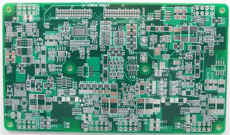
Detailed explanation of PCB proofing and electroplating
It is believed that those who understand the production process of pcb circuit board proofing know that electroplating is an indispensable and the most important part of circuit boards, because the success of electroplating directly affects whether the circuit boards are qualified. Why can't some circuit board factories guarantee the quality? Because electroplating is not well controlled and electroplating is not well done, there will be copper and no copper in the electroplating holes, which will affect whether the circuit is open or closed, Today, the pcbB circuit board manufacturer will explain the middle note of the electroplating process,
PCB proofing and electroplating additives include inorganic additives (such as CADmium salt for copper plating) and organic additives (such as coumarin for nickel plating). Most of the electroplating additives used in the early days were inorganic salts, and then organic substances gradually gained a leading position in the ranks of electroplating additives. According to the functional classification, electroplating additives can be divided into brighteners, leveling agents, stress relieving agents and wetting agents. Additives with different functions generally have different structural characteristics and action mechanisms, but multifunctional additives are also common. For example, saccharin can be used as both a nickel plating brightener and a commonly used stress reliever; And additives with different functions may also follow the same action mechanism.
1. Non proliferation control mechanism
According to the dominant non diffusion factors in electroplating, the non diffusion control mechanism of additives can be divided into electro adsorption mechanism, complex formation mechanism (including ion bridge mechanism), ion pair mechanism, mechanism of changing Helmholtz potential, mechanism of changing electrode surface tension, etc.
2. PCB proofing diffusion control mechanism
In most cases, the diffusion of additives to the cathode (rather than the diffusion of metal ions) determines the electrodeposition rate of metals. This is because the concentration of metal ions is generally 100~105 tiMES that of additives. For metal ions, the current density of electrode reaction is far lower than its limit current density.
Under the control of additive diffusion in PCB proofing, most additive particles diffuse and adsorb on the protrusions, active parts and special crystal planes with high electrode surface tension, causing the adsorbed atoms on the electrode surface to migrate to the depression on the electrode surface and enter the lattice, thus playing a role in leveling and brightening.


抖音二維碼

Q Q二維碼

微信二維碼
點擊
然后
聯(lián)系
然后
聯(lián)系
電話熱線
13410863085Q Q

微信

- 郵箱