鑫景福致力于滿足“快速服務,零缺陷,輔助研發”PCBA訂購單需求。


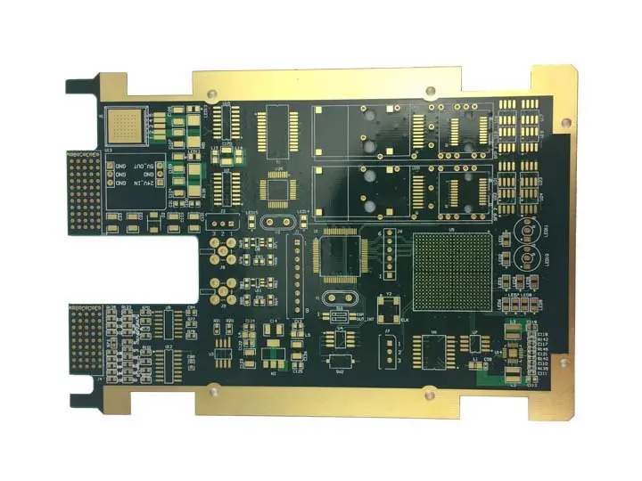
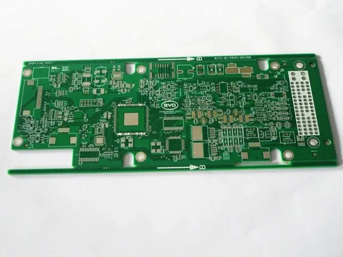
PCB制造
The Circuit board manufacturer will explain to you about the cost saving of PCB design assembly again?
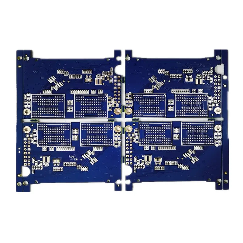
Number of panel units
How many unit boards should be included in a panel should be determined according to the actual situation. In principle, the more the number is, the better. The more the number is, the less the transmission time of a single PCB on the track is, and the higher the utilization rate of equipment is; At the same time, the greater the number of panels, the higher the utilization rate of materials used in PCB manufacturing, and the lower the cost. Of course, there is a limit. SometiMES, with the increase of the number of panels, the material cost of unit boards will rise, mainly because the equipment capacity of PCB manufacturers is limited. How many unit boards should be included in a panel may be considered from the following aspects:
1. Equipment capability, the maximum PCB size that the equipment can produce (print or mount). Within this maximum allowable size range, it is possible to include as many unit boards as possible.
2. PCB thickness. If the thICkness of PCB is SMAll, it is necessary to consider the deformation of the whole board during reflow or wave crest. Therefore, the panel size also needs to consider reducing the influence of PCB deformation on assembly quality.
3. Whether the fixture is used for auxiliary production. For PCB with small thickness, if the fixture is used for auxiliary production, the requirements for panel size can also be relaxed, but this may involve cost growth.
4. Whether the production operation is easy or not, and whether the size is too large may cause operational safety problems, which also need to be considered.
An appropriate connection shall be designed between the unit boards inside the panel and between the unit board and the process edge, which can not only ensure sufficient strength support during the production process, but also consider that after the assembly is completed, the operation of cutting the process edge and the connection point is SIMple and easy, and will not cause other quality problems.
There are generally three types of connection point design: V-Scoring, stamp hole and conventional connection. The method to be adopted depends on the production capacity of the equipment: if there is no automatic plate dividing equipment but only manual plate dividing is adopted, V-Scoring or stamp hole connection can be considered; If the mechanical equipment plate splitting process is adopted, any design can be adopted.
1. V-Scoring design: the angle is usually kept at 30 °, 45 ° or 60 °, and the reserved thickness of the notch center is generally 0.5mm, which can be trimmed according to the actual situation. If the shape of the panel is large, and the components on the panel are heavy, the production may be affected due to the fracture of the process edge. The thickness can be increased appropriately. On the contrary, if there is no such concern, the assembly will be affected by the excessive burr of the sub plate, and the thickness can also be appropriately reduced.
2. The design size, aperture and hole spacing of stamp holes are the same as V-Scoring, which is generally used for manual plate splitting design. It is necessary to consider the sufficient strength in the production and assembly process and the simplicity of plate splitting.
3. Generally speaking, the common connection design has no strength concerns, and only needs to consider the subsequent plate division problem. This connection needs to use mechanical equipment for auxiliary analysis, such as Punch, Router, etc., It is mainly necessary to consider the efficiency of subsequent sub boards.
Other design rules:
1. A 1.6mm or 2.4mm interval shall be reserved between each unit board in the panel to facilitate the division of Router or Punch. If a width less than 1.6mm is adopted, it is necessary to consider whether the equipment is suitable for such small gaps.
2. On the four corners of the panel, design the tool holes that do not need plating. The entire panel shall ensure at least two holes, with the hole size of 3.05 ± 0.05mm. The center of the hole should be positioned at the corner of PCB, 5mm in X and Y directions respectively.
3. Fillets or chamfers with a radius of 5mm shall be designed on the four corners of the panel to prevent jamming on the rail transmission belt.
4. The panel design must ensure that the distance between the edge of the reference point (including the green oil opening) and the panel edge is at least 5mm. The reference points on both sides should not be placed symmetrically, so that PCB can be prevented from entering the machine in reverse through the identification function of the device itself.
5. A direction sign can be designed at the edge of the panel, such as the sEMIcircle hole at the edge, to prevent PCB from being in the wrong direction during production.
6. The maximum contour tolerance of PCB assembly shall be controlLED within 0.05mm.
3. Data required for completion of panel design
If you want to design a good panel drawing, you must have enough information to support it, otherwise it may cause subsequent SMT assembly or panel splitting quality problems due to unreasonable panel design. To complete a qualified panel design, the following data information is usually required.
Gerber file, including PCB component distribution, considering panel spacing and connection point placement position;
Outline drawing of PCB to understand the overall dimensions and specifications of PCB;
The specification of large components, especially plate edge components, requires the design of panel spacing, avoidance, etc.
4. Impact of poor panel design on production
In practical work, there are often some problems in panel design for various reasons, which may lead to production failure and difficulty in panel splitting.
The components at the edge of the board cannot be installed normally without the avoidance design;
The distance between the unit plates is too small, causing difficulty in mold manufacturing or easy damage to the tool;
If the process edge is too narrow, the solder paste or components close to the plate edge will be erased during rail transmission;
Poor welding due to excessive panel size and high temperature deformation;
Insufficient process edges or few connection points lead to insufficient rigidity of the panel and affect production.
5. Summary
The above is mainly about the design requirements for rigid pcb assembly. For flexible FPC, the requirements for assembly may be different due to different production methods. In any case, the panel design is to meet the SMT assembly requirements and safe operation. After the assembly is completed, it will return to the finished veneer assembly. Therefore, regardless of hard board or soft board, both the assembly strength requirements and the splitting requirements after the production are considered in the panel design. Meeting these two points is a good panel design.


抖音二維碼

Q Q二維碼

微信二維碼
點擊
然后
聯系
然后
聯系
電話熱線
13410863085Q Q

微信

- 郵箱